Touch panel and manufacturing method thereof, and touch display device

A touch panel and touch area technology, applied in circuit devices, programmable/customizable/modified circuits, printed circuits, etc., can solve problems such as poor products, no solutions provided, weak signals, etc., and improve product quality. Yield, the effect of improving ESD resistance

Inactive Publication Date: 2016-12-07
BOE TECH GRP CO LTD +1
View PDF5 Cites 14 Cited by
  • Summary
  • Abstract
  • Description
  • Claims
  • Application Information

AI Technical Summary

Problems solved by technology

Rx is used as the receiving electrode, its signal is weak, and it is easy to cause product failure when a small-a

Method used


Image

  • Touch panel and manufacturing method thereof, and touch display device
  • Touch panel and manufacturing method thereof, and touch display device
  • Touch panel and manufacturing method thereof, and touch display device

Examples


Embodiment Construction

[0029] The following will clearly and completely describe the technical solutions in the embodiments of the present invention with reference to the accompanying drawings in the embodiments of the present invention. Obviously, the described embodiments are only part of the embodiments of the present invention, not all of them. Based on the embodiments of the present invention, all other embodiments obtained by persons of ordinary skill in the art without making creative efforts belong to the protection scope of the present invention.

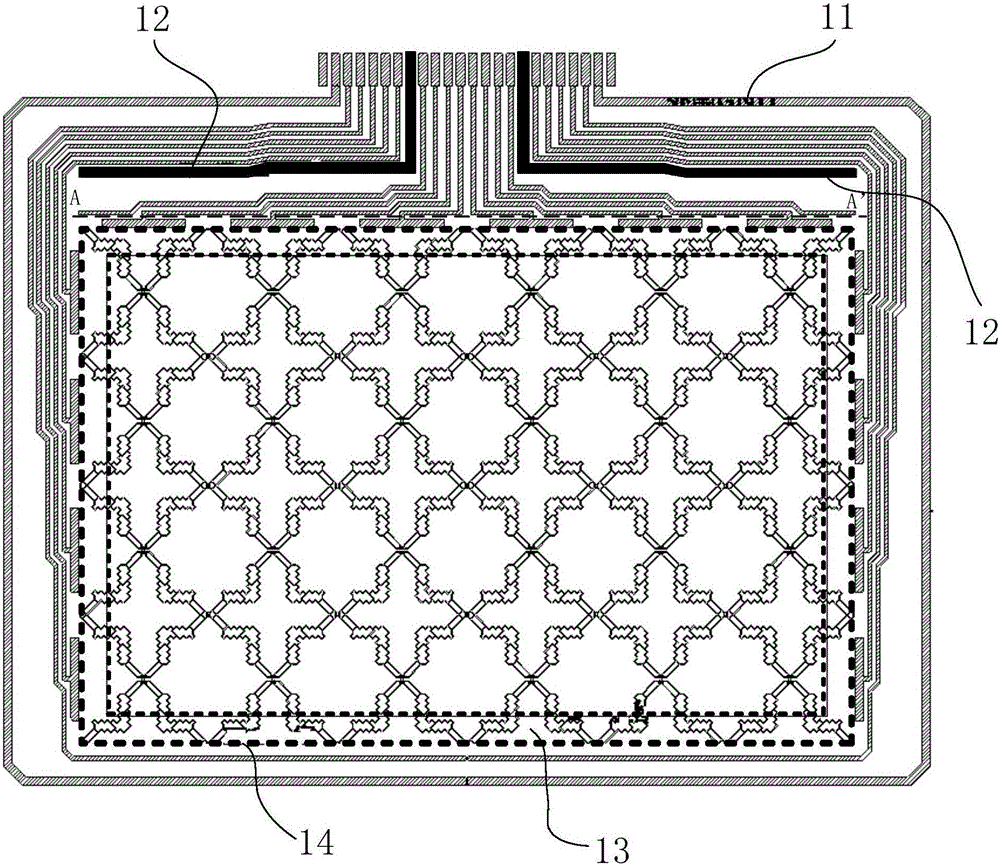
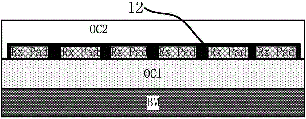
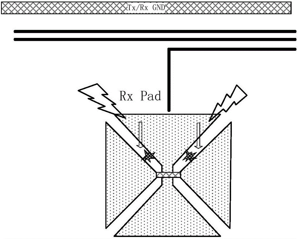
[0030] figure 1 It is a schematic diagram of the ground wire structure of the touch screen according to the prior art, such as figure 1 As shown, there are three ground wires (GND wires) in the touch screen. Among them, the peripheral ground wire 11 of the touch screen is a loop, which can conduct away the static electricity on the edge of the touch screen. Secondly, the driving electrodes (Tx) and sensing electrodes (Rx) There are also two grou...


PUM


Abstract

The invention discloses a touch panel and a manufacturing method thereof, and a touch display device. The touch panel comprises a touch area and a routing area, wherein the routing area surrounds the touch area; the routing area comprises a drive electrode routing and an induction electrode routing; a first ground routing in a loop state surrounds the induction electrode routing, and has an overlapping area with the induction electrode routing; and the first ground routing can lead static electricity generated by the touch panel to the outside. Through the touch panel and the manufacturing method thereof, and the touch display device disclosed by the invention, the static electricity gathered at the edges of a black matrix and a position of an induction electrode can be led out; and thus, the effect of preventing the static electricity from breaking through the BM to cause product badness is achieved.

Description

technical field [0001] The present invention relates to the field of display technology, in particular to a touch panel, a manufacturing method thereof, and a touch display device. Background technique [0002] In recent years, with the improvement of the controllability of mobile electronic devices and the development of electronic technology, touch screen technology has been widely used in electronic devices such as mobile phones, tablets, and notebook computers. The development of touch technology has emerged in different technical directions such as resistance, capacitance, and electromagnetics. Among them, capacitive screens have become mainstream products due to their low cost and better user experience. [0003] ESD (Electro-Static Discharge, electrostatic discharge) may cause the performance of the device to deteriorate, or break down the device to cause permanent failure of the device, such as an open circuit or short circuit inside the device. In the manufacturing...

Claims


Application Information

Patent Timeline
IPC IPC(8): G06F3/041G06F3/044
CPCG06F3/0412G06F3/044G06F2203/04103G06F2203/04112G06F2203/04111G06F3/04164G06F3/0443G06F3/0446H05K1/0259H05K1/0289H05K2201/10128G06F3/0488
Inventor 王庆浦张雷石高亮吴锦熹
Owner BOE TECH GRP CO LTD
Why Eureka
Try Eureka