Touch substrate, manufacture method thereof, and touch screen
A manufacturing method and a technology of a touch screen, which are applied in the field of a touch substrate and its manufacture, and a touch screen, can solve the problems of black matrix pattern resistivity reduction, permanent failure, and open circuit of electrode blocks, so as to improve ESD resistance, The effect of reducing the risk of breakdown and improving the breakdown voltage
- Summary
- Abstract
- Description
- Claims
- Application Information
AI Technical Summary
Problems solved by technology
Method used
Image
Examples
Embodiment 1
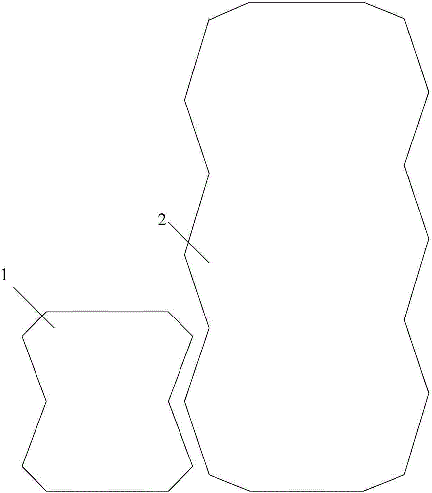
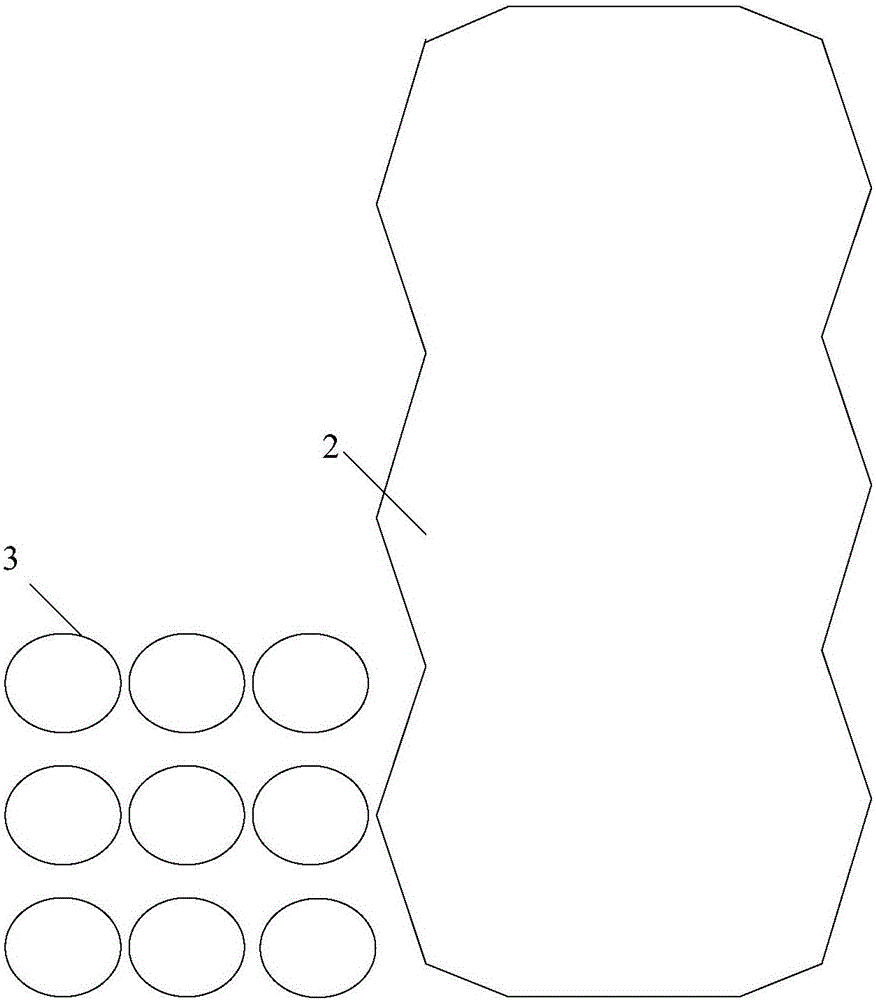
[0036] This embodiment provides a touch control substrate, including a touch control area and a black matrix pattern surrounding the touch control area. A plurality of touch electrodes are arranged on the touch control substrate, and each touch control electrode between adjacent touch control electrodes A dummy electrode pattern is formed in the gap, and each dummy electrode pattern between the touch electrodes overlapping on the black matrix pattern is composed of a plurality of mutually insulated dummy electrode blocks.
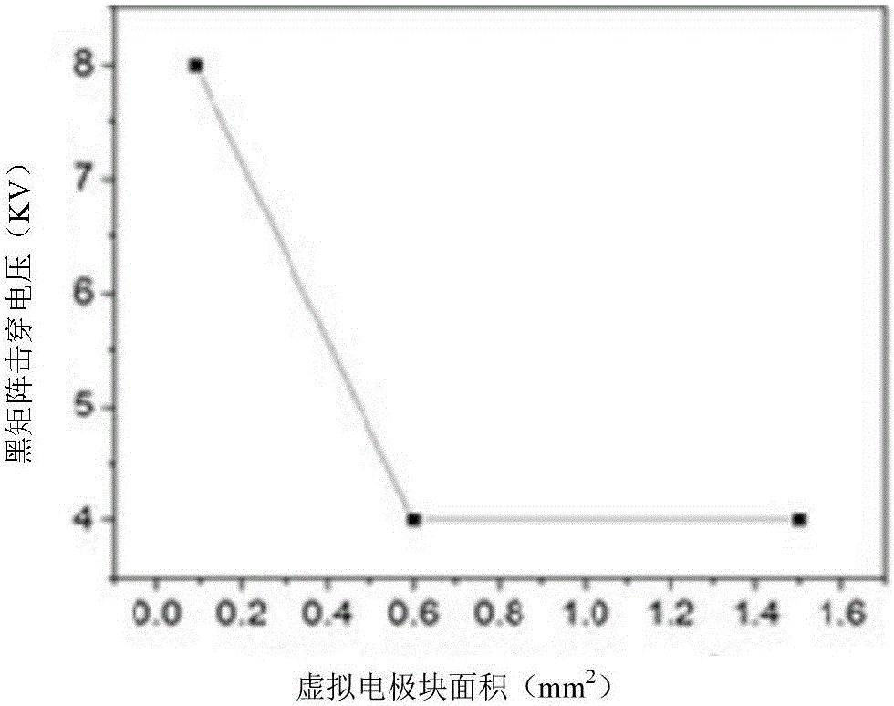
[0037] Since ESD is prone to occur between the touch electrodes overlapping the black matrix pattern and the adjacent dummy electrode patterns, and after a large number of experimental verifications, it is found that after the area of the dummy electrode block decreases, the gap between the touch electrode and the dummy electrode block The breakdown voltage of the black matrix pattern is greatly improved. Therefore, in this embodiment, each virtual electro...
Embodiment 2
[0051] This embodiment provides a touch screen, including the above-mentioned touch substrate. The touch screen can be applied in human-computer interaction devices.
Embodiment 3
[0053] This embodiment provides a method for manufacturing a touch substrate. The touch substrate includes a touch area and a black matrix pattern surrounding the touch area. The touch substrate is provided with a plurality of touch electrodes. A dummy electrode pattern is formed at each gap between adjacent touch electrodes, and the manufacturing method includes:
[0054] A dummy electrode pattern is formed between the touch electrodes overlapping the black matrix pattern, and each dummy electrode pattern is composed of a plurality of dummy electrode blocks insulated from each other.
[0055] Since ESD is prone to occur between the touch electrodes overlapping the black matrix pattern and the adjacent dummy electrode patterns, and after a large number of experimental verifications, it is found that after the area of the dummy electrode block decreases, the gap between the touch electrode and the dummy electrode block The breakdown voltage of the black matrix pattern is grea...
PUM
 Abstract
Description
Claims
Application Information
 - R&D
- Intellectual Property
- Life Sciences
- Materials
- Tech Scout
- Unparalleled Data Quality
- Higher Quality Content
- 60% Fewer Hallucinations
Browse by: Latest US Patents, China's latest patents, Technical Efficacy Thesaurus, Application Domain, Technology Topic, Popular Technical Reports.
© 2025 PatSnap. All rights reserved.Legal|Privacy policy|Modern Slavery Act Transparency Statement|Sitemap|About US| Contact US: help@patsnap.com


