
A kind of vdmos device and its making method

A manufacturing method and device technology, which is applied in semiconductor/solid-state device manufacturing, semiconductor devices, electrical components, etc., can solve the problems of easy failure of EAS and achieve the effect of improving EAS capability

Active Publication Date: 2019-08-06
FOUNDER MICROELECTRONICS INT
View PDF4 Cites 0 Cited by
  • Summary
  • Abstract
  • Description
  • Claims
  • Application Information

AI Technical Summary

Problems solved by technology

[0006] The purpose of the present invention is to provide a VDMOS device and its manufacturing method, in order to solve the problem that the EAS of the existing VDMOS device is easy to fail

Method used

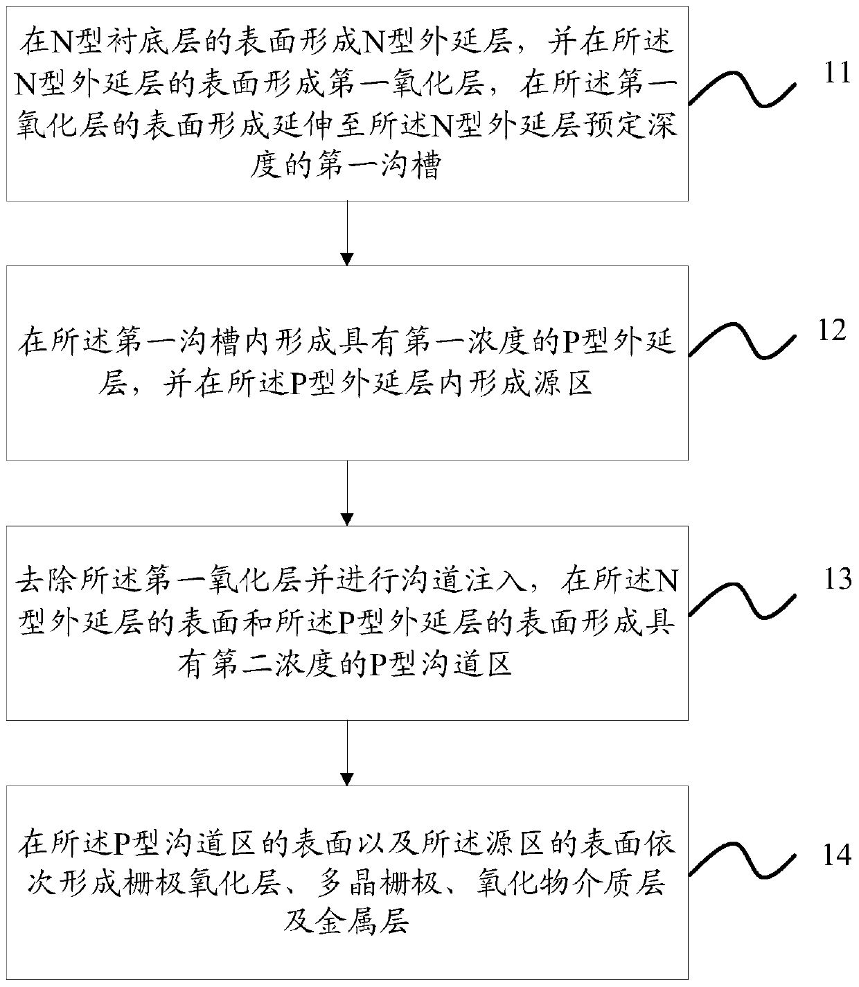
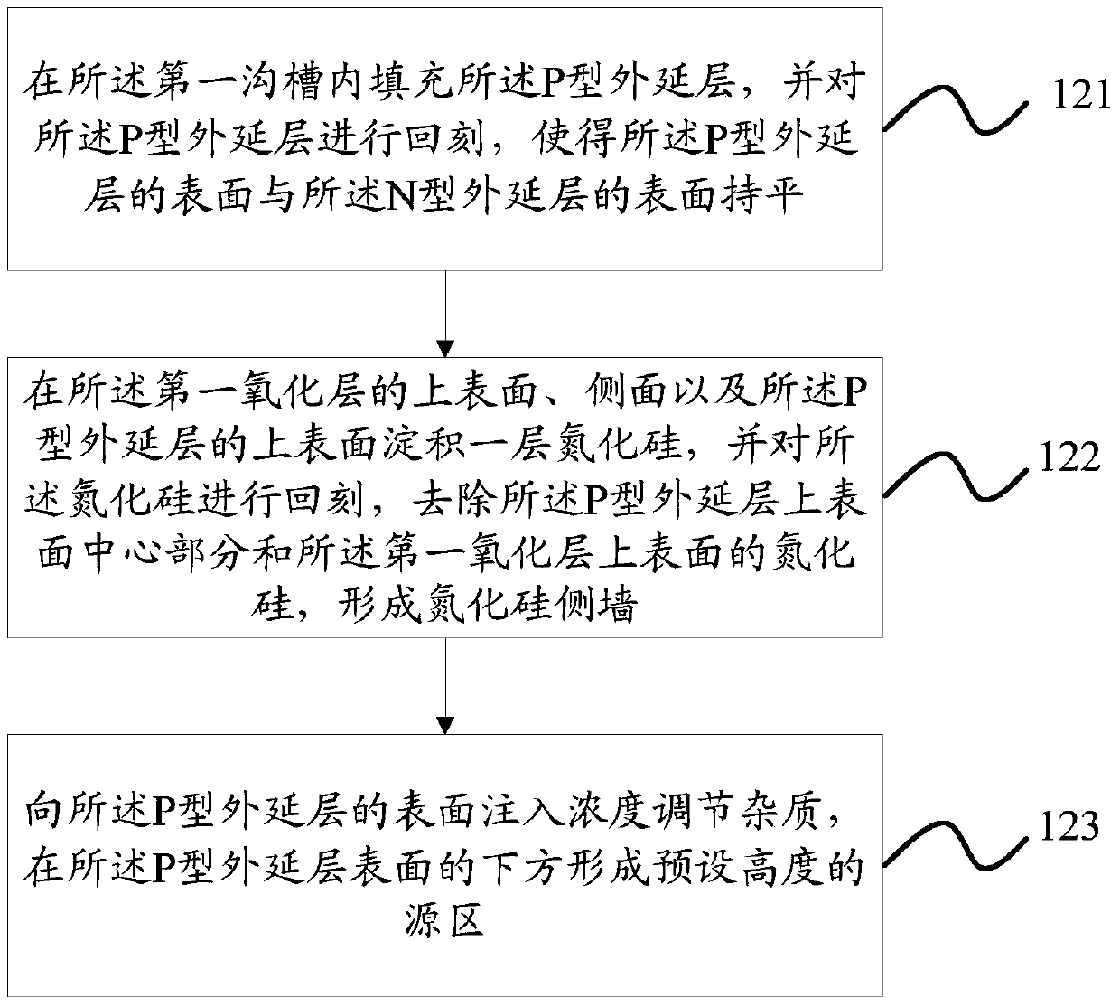

Image

  • A kind of vdmos device and its making method
  • A kind of vdmos device and its making method
  • A kind of vdmos device and its making method

Examples


Embodiment Construction

[0054] In order to make the technical problems, technical solutions and advantages to be solved by the present invention clearer, the following will describe in detail with reference to specific embodiments and accompanying drawings.

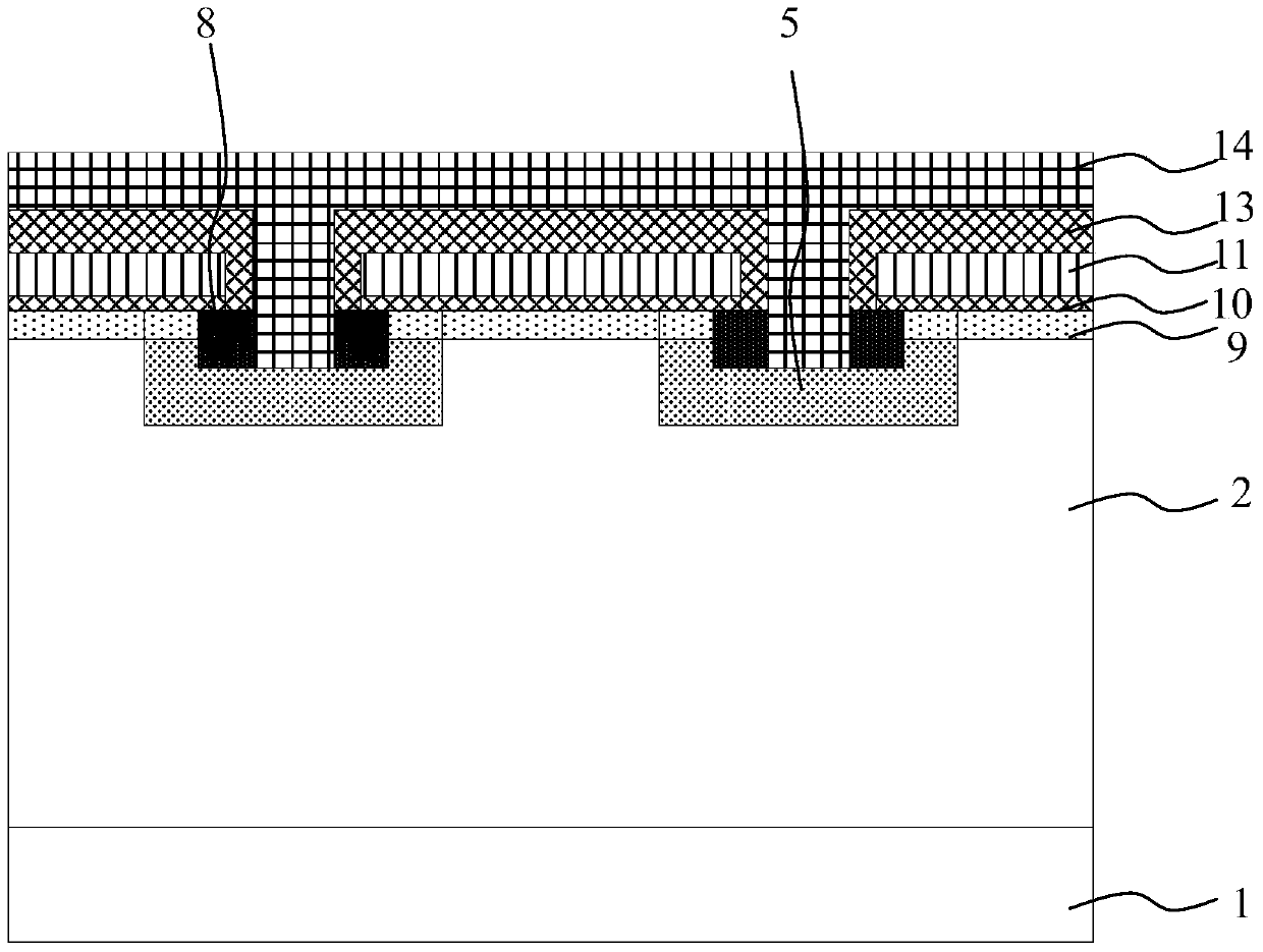
[0055] The embodiment of the present invention solves the problem that the EAS of the existing VDMOS device is prone to failure. The embodiment of the present invention provides a VDMOS device, such as figure 1 shown, including:

[0056] N-type substrate layer 1; an N-type epitaxial layer 2 located on the surface of the N-type substrate layer 1, and a first groove 4 is arranged on the N-type epitaxial layer 2, and a gate located on the N-type epitaxial layer 2 Extreme oxide layer 10, polycrystalline gate 11, oxide dielectric layer 13 and metal layer 14, the VDMOS device also includes:

[0057] A P-type epitaxial layer 5 with a first concentration disposed in the first trench 4, an active region 8 is embedded in the P-type epitaxial layer 5, and t...


PUM


Abstract

The invention provides a VDMOS (Vertical double diffused metal oxide semiconductor) device and a manufacturing method thereof, which relate to the field of semiconductor chip manufacturing, and aim at solving the problem that EAS (Single Pulsed Avalanche Energy) of the existing VDMOS device is likely to fail. The VDMOS device comprises an N-type substrate layer, an N-type epitaxial layer located on the surface of the N-type substrate layer, a first groove arranged in the N-type epitaxial layer, and a gate oxide layer, a polycrystalline gate, an oxide dielectric layer and a metal layer located on the N-type epitaxial layer, a P-type epitaxial layer with a first concentration arranged in the first groove, a source region whose surface is higher than the surface of the N-type epitaxial layer and embedded in the P-type epitaxial layer, a second groove arranged in the source region and communicated to a metal layer, and a P-type channel region with a second concentration located between the N-type epitaxial layer and the gate oxide layer and arranged in a region out of the source region and the second groove. The surface of the source region is flush with that of the P-type channel region. The EAS ability of the device can be effectively enhanced.

Description

technical field [0001] The invention relates to the field of semiconductor devices, in particular to a VDMOS device and a manufacturing method thereof. Background technique [0002] VDMOS (Vertical double diffused metal oxide semiconductor, vertical double diffused metal oxide semiconductor field effect transistor) device has a very important parameter, EAS (Single Pulsed Avalanche Energy, single pulse avalanche energy), which is defined as the energy consumed by the device in a single avalanche state maximum energy. In applications where large voltage spikes are generated at the source and drain, the avalanche energy of the device must be considered. EAS capability is also a very important parameter to measure VDMOS devices. [0003] There are two modes of EAS failure of general devices, thermal damage and conduction damage of parasitic transistors. The conduction damage of the parasitic triode means that there is a parasitic triode (epitaxial layer-body region-source re...

Claims


Application Information

Patent Timeline
Patent Type & Authority Patents(China)
IPC IPC(8): H01L29/78H01L21/336
Inventor 赵圣哲
Owner FOUNDER MICROELECTRONICS INT
Learn More