A kind of MOS tube and its manufacturing method

A manufacturing method and technology for MOS transistors, which are used in semiconductor/solid-state device manufacturing, semiconductor devices, electrical components, etc., can solve problems such as low EAS and complex processes, and achieve the effect of improving EAS capabilities.

Active Publication Date: 2019-04-09
FOUNDER MICROELECTRONICS INT
View PDF5 Cites 0 Cited by
  • Summary
  • Abstract
  • Description
  • Claims
  • Application Information

AI Technical Summary

Problems solved by technology

However, this method also needs to precipitate Spacer when injecting P+, the process is complicated, and the EAS is low

Method used


Image

  • A kind of MOS tube and its manufacturing method
  • A kind of MOS tube and its manufacturing method
  • A kind of MOS tube and its manufacturing method

Examples


Embodiment Construction

[0059] In order to make the technical problems, technical solutions and advantages to be solved by the present invention clearer, the following will describe in detail with reference to the drawings and specific embodiments.

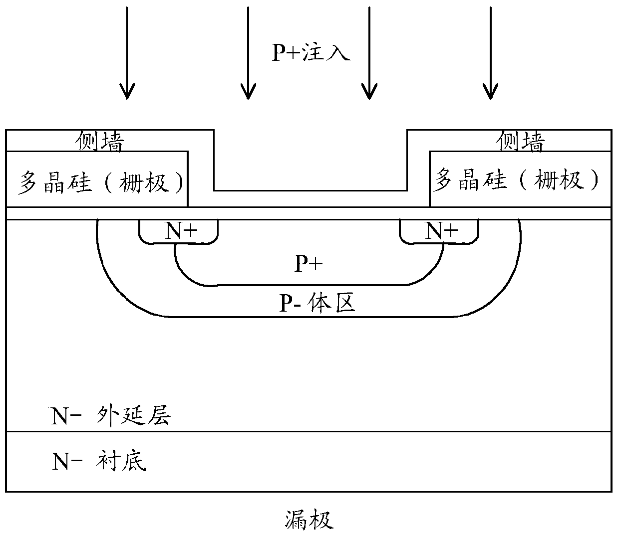
[0060] The present invention aims at the existing process of manufacturing MOS tubes. When injecting P+, Spacer needs to be precipitated, the process is complicated, and as the problem of low impact resistance of switches, a method for manufacturing MOS tubes is provided, which directly utilizes the method of self-alignment. P+ injection to get better EAS capability.

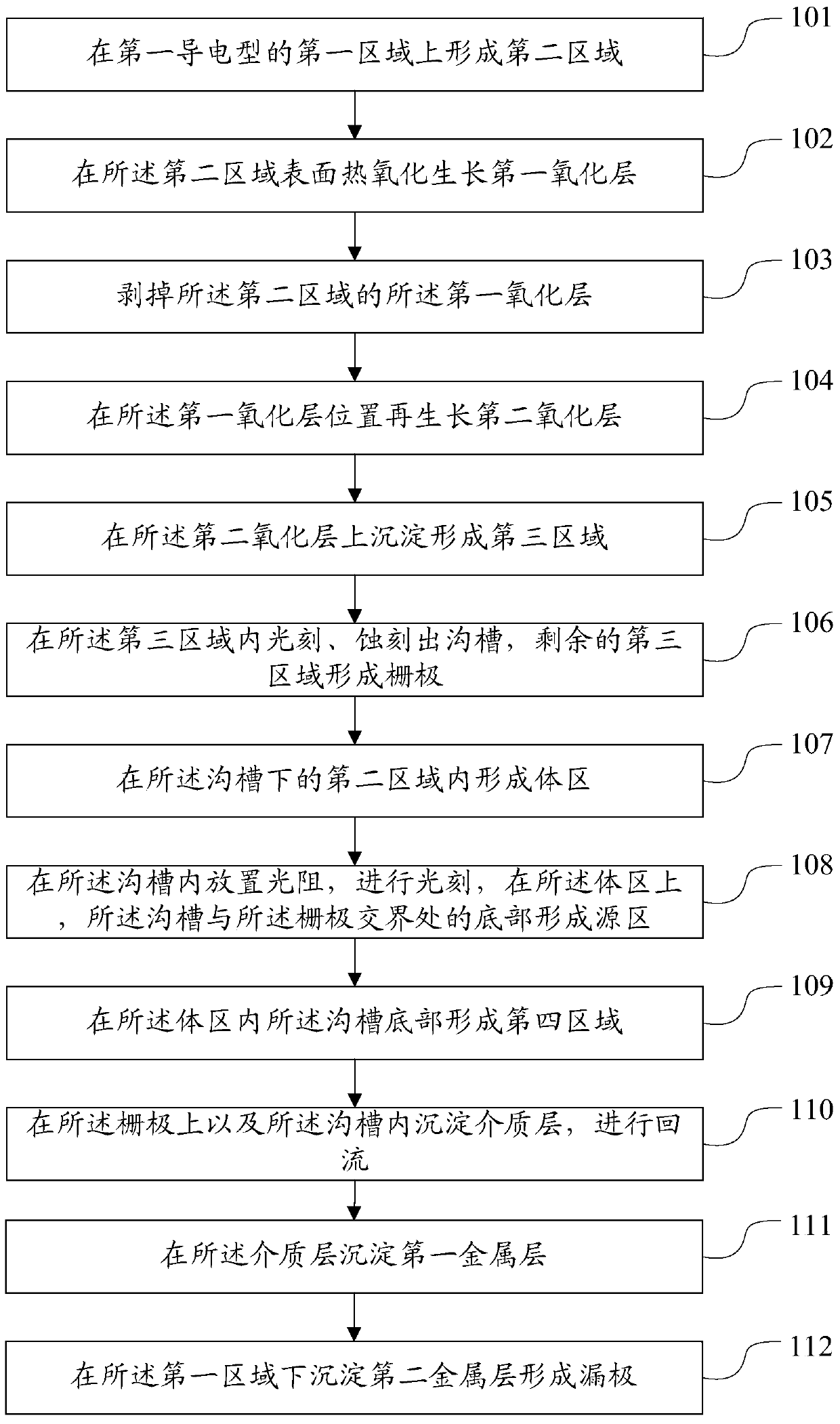
[0061] Such as figure 2 As shown, a method for manufacturing a MOS tube according to an embodiment of the present invention includes the following steps:

[0062] Step 101, forming a second region on the first region of the first conductivity type;

[0063] Step 102, growing a first oxide layer by thermal oxidation on the surface of the second region;

[0064] Step 103, peeling off the...


PUM


Abstract

The invention provides a MOS tube and a manufacture method thereof, and relates to the technical field of a semiconductor. The method comprises the following steps: forming a second area on a first area of a first conductive type; growing a first oxide layer on the surface of the second area through thermal oxidization; stripping the first oxide layer of the second area; re-growing a second oxide layer at the position of the first oxide layer; performing precipitation to form a third area on the second oxide layer; performing photoetching to etch a groove in the third area, and forming a grid in the residual third area; forming a body region in the second area below the groove; placing a light resistor in the groove, performing photoetching, and forming a source region at the bottom of the juncture of the groove and the grid on the body region; forming a fourth area at the bottom of the groove in the body region; depositing a dielectric layer on the grid and in the groove, and performing backflow; depositing a first metal layer at the dielectric layer; and depositing a second metal layer under the first area to form a drain electrode. The method provided by the invention solves the problem of low anti-impact capability of a MOS tube which is manufactured by use of a conventional manufacture process and is taken as a switch.

Description

technical field [0001] The invention relates to the technical field of semiconductors, in particular to a MOS transistor and a manufacturing method thereof. Background technique [0002] Planar DMOS tube is one of the most typical semiconductor devices, and it is currently widely used in circuits such as power adapters, inverters, xenon lamps, and LED drivers. [0003] In the manufacturing technology of high-voltage DMOS tubes, the single-pulse avalanche breakdown energy EAS reflects the impact resistance of the device as a switch, and is a measure of the level at which the device can safely absorb reverse avalanche energy. Therefore, it is very important to improve the EAS impact resistance of the device . General traditional methods such as figure 1 As shown, the side wall (Spacer) blocking process is used, and a layer of Spacer is deposited first, and then P+ is injected. Depending on the specific situation, the back-engraving process can also be selected. However, thi...

Claims


Application Information

Patent Timeline
Patent Type & Authority Patents(China)
IPC IPC(8): H01L21/336H01L21/266H01L29/78
CPCH01L21/266H01L29/66477H01L29/78
Inventor 蔡远飞何昌姜春亮
Owner FOUNDER MICROELECTRONICS INT
Why Eureka
Try Eureka