Super junction device

A superjunction device and charge technology, applied in the field of semiconductor integrated circuits, can solve the problems of reducing EAS capability, EAS burning, reducing parasitic triode base current, etc., to avoid high electric field damage, simple electric field distribution, and saving chip size.

Pending Publication Date: 2020-11-03
SHANGHAI HUAHONG GRACE SEMICON MFG CORP
View PDF0 Cites 0 Cited by
  • Summary
  • Abstract
  • Description
  • Claims
  • Application Information

AI Technical Summary

Problems solved by technology

[0006] Since the parasitic triode will be turned on when the base current of the parasitic triode is large, thereby reducing the EAS capability, so in order to improve the EAS capability of the device, it is usually necessary to guide the avalanche current path away from the base region of the parasitic triode, thereby reducing the base of the parasitic triode. area current; in addition, the existing super-junction devices are very prone to EAS burnout at the corner of the terminal or near the terminal, which is a big bottleneck for improving the overall EAS capability

Method used


Image

  • Super junction device
  • Super junction device
  • Super junction device

Examples


Embodiment Construction

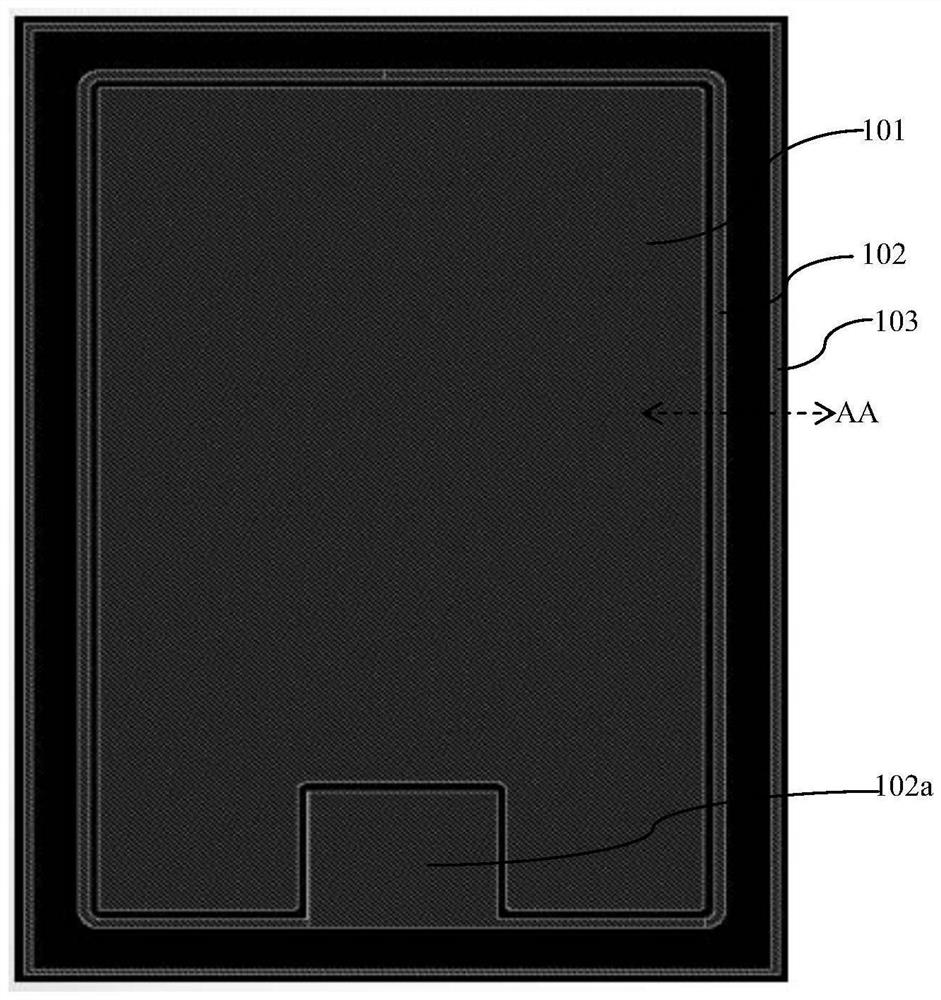
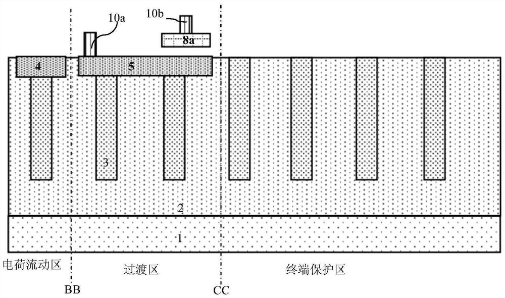
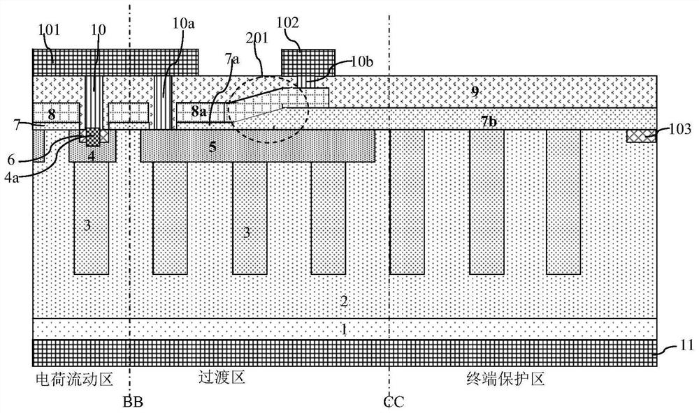
[0048] The technical solution of the embodiment of the present invention is obtained on the basis of analyzing the existing technical problems. Before introducing the technical solution of the embodiment of the present invention in detail, the structure of the existing super-junction device is described as follows, as follows figure 1 Shown is a schematic diagram of the layout structure of the existing super junction device; figure 2 yes figure 1 Schematic diagram of the cross-sectional structure of the device at the position of the AA line; image 3 yes figure 2 Schematic diagram of the cross-sectional structure of the device when the middle gate structure is a planar gate; the middle region of the existing super-junction device is the charge flow region, the terminal protection region is formed around the charge flow region, and the transition region is located between the terminal protection region and the between the charge flow regions, figure 2 In , the left side o...


PUM


Abstract

The invention discloses a super junction device, a P-type ring is formed in a transition region, and a layout structure comprises a gate bus composed of a front metal layer, a gate liner and a sourcemetal layer; the gate bus and the gate liner are surrounded by the source metal layer; the gate bus is completely located above the region of the charge flow region; the P-type ring surrounds the gatebus and the gate liner; the source electrode metal layer covers the grid electrode bus and the charge flowing region outside the grid electrode liner and extends to the upper part of the P-type ring;each gate conductive material layer is connected to the corresponding gate bus or gate liner through a first contact hole, a plurality of second contact holes connected to the source metal layer areformed in the P-type ring, and a non-intersection structure between the gate conductive material layer and the P-type ring enables the second contact holes to be formed in each area of the top of theP-type ring. According to the invention, the EAS capability and the UIS capability of the device can be improved, the gate structure can be prevented from being damaged by a high electric field, and the chip size can be effectively saved.

Description

technical field [0001] The invention relates to a semiconductor integrated circuit, in particular to a super junction device. Background technique [0002] The super-junction MOSFET adopts a new voltage-resistant layer structure, and uses a series of superjunction structures composed of alternately arranged semiconductor P-type thin layers and N-type thin layers to combine P-type thin layers and N-type thin layers at lower voltages in the off state. The N-type thin layer is depleted to achieve mutual compensation of charges, so that the P-type thin layer and N-type thin layer can achieve high breakdown voltage under high doping concentration, thereby obtaining low on-resistance and high reverse breakdown at the same time Voltage (BV), that is, super junction MOSFET is to use PN, that is, P-type thin layer and N-type thin layer charge balance to reduce the surface electric field (Resurf) technology in the body to improve the BV of the device while maintaining a small on-resis...

Claims


Application Information

Patent Timeline
IPC IPC(8): H01L29/423H01L29/78H01L29/06
CPCH01L29/7802H01L29/0634H01L29/4238H01L29/42376
Inventor 李昊
Owner SHANGHAI HUAHONG GRACE SEMICON MFG CORP
Why Eureka
Try Eureka