High-voltage-resistant SGT device

A technology of high withstand voltage and devices, which is applied in the direction of semiconductor devices, electric solid devices, electrical components, etc., can solve the problem of lower breakdown voltage, lower breakdown withstand voltage BV at the corner of the cell trench 1 end, and reliability of SGT devices And EAS capacity reduction and other issues, to achieve the effect of improving the pressure resistance

Pending Publication Date: 2022-07-29
江苏芯长征微电子集团股份有限公司 +1
View PDF0 Cites 0 Cited by
  • Summary
  • Abstract
  • Description
  • Claims
  • Application Information

AI Technical Summary

Problems solved by technology

When the mesa width between the end of the cell trench 1 in the active region and the adjacent terminal inner ring 23 is consistent with the mesa width between the cell trench 1 in the active region, then the end corner of the cell trench 1 The width of the mesa between the inner ring 22 and the adjacent terminal will be too large, resulting in a decrease in the breakdown voltage BV at the end corner of the cell trench 1; on the other hand, when reducing the When the mesa width between the rings 22, although it can be ensured that the mesa width at the end corner of the cell trench 1 is basically the same as the mesa width between the adjacent cell trenches 1 in the active region, because the cell trench 1 The width of the mesa between the terminal and the inner ring 2 adjacent to the terminal is reduced, where the breakdown voltage BV will be reduced
[0006] Therefore, according to the two-dimensional design method of the transition region 3 of the traditional cell terminal, it is impossible to achieve the same breakdown voltage BV of the transition region and the active region, resulting in a low breakdown voltage BV breakdown point at the terminal, which further leads to the reliability of the SGT device. The performance and EAS capability are reduced, which cannot meet the high withstand voltage requirements of SGT devices

Method used


Image

  • High-voltage-resistant SGT device
  • High-voltage-resistant SGT device
  • High-voltage-resistant SGT device

Examples


Embodiment Construction

[0031] The present invention will be further described below with reference to the specific drawings and embodiments.

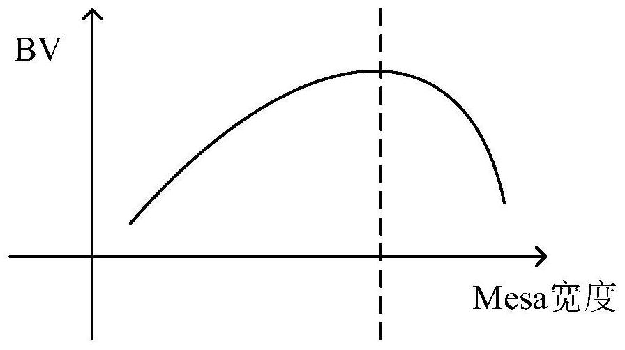
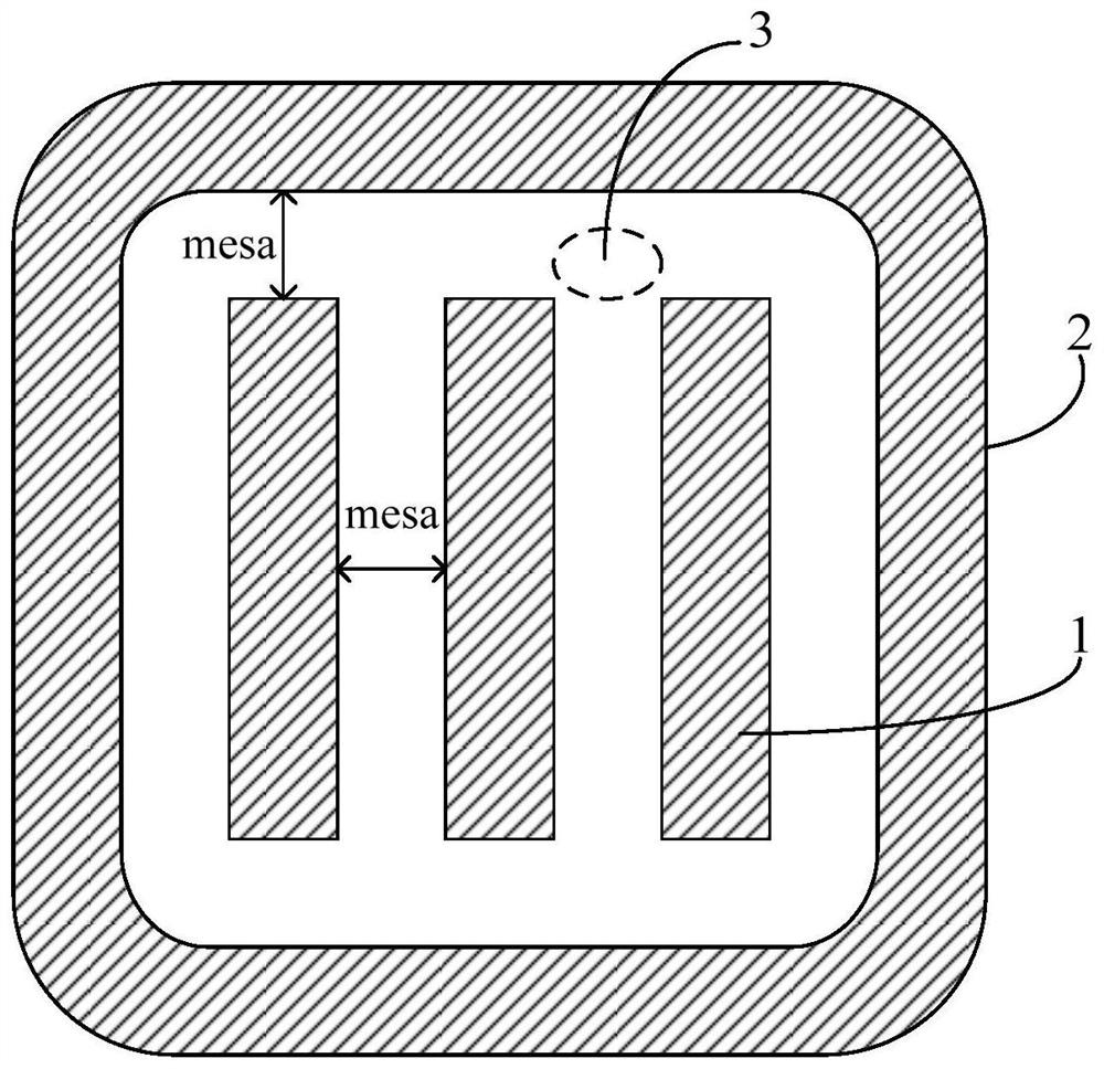
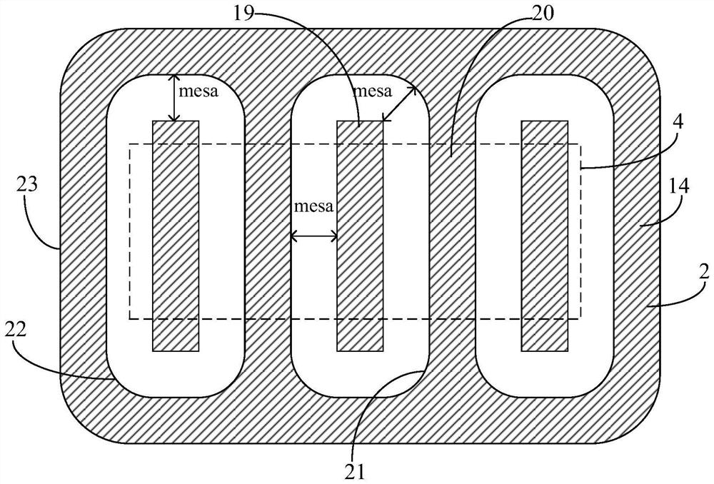
[0032] like image 3 Shown: In order to improve the withstand voltage capability, EAS capability and reliability of the SGT device, the present invention includes a semiconductor substrate, an active region 4 prepared in the central region of the semiconductor substrate, and a terminal for protecting the active region 4 area 2; the active area 4 includes a number of cells distributed in parallel, and the cells in the active area 4 adopt the SGT structure; the terminal area 2 at least includes a terminal inner ring 23 adjacent to and surrounding the active area 4, the The terminal inner ring 23 includes the terminal ring groove 14;

[0033] On the top plan view of the SGT device, the cells in the active region 4 are elongated, and along the direction perpendicular to the length of the cells, the active region 4 includes a plurality of first cell units 19 alte...


PUM


Abstract

The invention relates to a high-voltage-resistant SGT device. Two end parts of a cellular groove in a second cellular unit are respectively connected with a terminal ring groove which is right corresponding to a terminal inner ring, and a cellular terminal groove combination part is formed at the connection part of the end part of the cellular groove in the second cellular unit and the terminal ring groove; for a first cellular unit and a second cellular unit which are adjacent to each other, the area width between the cellular groove in the first cellular unit and the cellular groove in the second cellular unit is mesa first width; the width of a region between the end part of the cellular groove in the first cellular unit and the corresponding terminal inner ring is an mesa second width, and the width of a region between the end corner of the end part of the cellular groove in the first cellular unit and the joint part of the corresponding cellular terminal groove and/or the transition part of the terminal ring groove is an mesa third width. The third width of the mesa and the second width of the mesa are consistent with the first width of the mesa. According to the invention, the voltage endurance capability, the EAS capability and the reliability of the SGT device can be improved.

Description

technical field [0001] The invention relates to a power semiconductor device, in particular to a high withstand voltage SGT device. Background technique [0002] At present, most of the drift regions of existing MOSFET devices only contain epitaxial layers without other structures. The drift region withstand voltage BV and on-resistance RDSON have a trade-off relationship between the silicon limit. In order to break through the performance limitations of traditional trench MOSFET devices, shielded gate transistors (SGTs) came into being. The main difference between SGT devices and existing power semiconductor devices is that a shielded gate structure is introduced into the drift region, and the shielded gate structure is used to deplete the drift region between the trenches through a lateral electric field, so that the mesa region between the trenches in the drift region can be Using a higher doping concentration further reduces the on-resistance and breaks through the sili...

Claims


Application Information

Patent Timeline
Patent Type & Authority Applications(China)
IPC IPC(8): H01L27/088H01L27/02H01L29/06H01L29/423
CPCH01L27/088H01L27/0207H01L29/0615H01L29/4236
Inventor 杨飞吴凯张广银徐真逸任雨
Owner 江苏芯长征微电子集团股份有限公司
Why Eureka
Try Eureka