Optoelectronic module for contactless optical link, related multi-channel modules, interconnection system, and associated method for manufacturing and connecting to a card
一种光电模块、多通道的技术,应用在印刷电路制造、电磁波传输系统、提供连接器和印刷电路板等方向,能够解决多占用空间等问题,达到减小占用空间、减小模块尺寸的效果
- Summary
- Abstract
- Description
- Claims
- Application Information
AI Technical Summary
Problems solved by technology
Method used
Image
Examples
Embodiment Construction
[0091] Throughout this application, the terms "vertical", "lower", "higher", "bottom", "top", "under" are understood with reference to the stacking direction of the individual components of the photovoltaic module according to the invention ,"above".
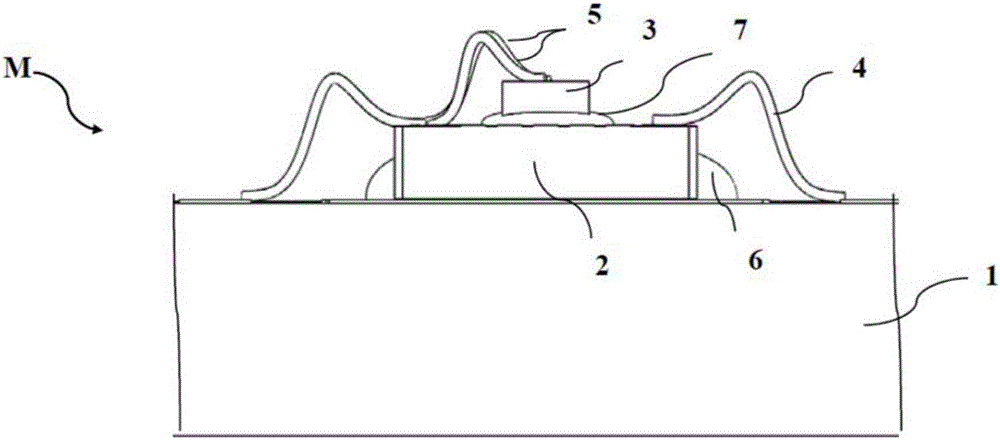
[0092] exist figure 1 A photovoltaic module M according to the invention is shown in .
[0093] The individual elements of the module M are stacked on top of each other and attached to each other, preferably by gluing, for example by means of epoxy glue, or by soldering.
[0094] Thus, from bottom to top of the stack, module M consists of:
[0095] - a printed circuit 1 which will act as an interface with the electronic application board;
[0096] - an electronic control part 2 attached directly to the printed circuit 1 and electrically connected to the electronic circuit by wires 4 soldered according to "wire-bonding" or bridging techniques;
[0097] - an optoelectronic component 3, adapted to transmit or receive light sign...
PUM
 Abstract
Description
Claims
Application Information


