Method for preparing transmission electron microscope sample

An electron microscope and sample technology, which is applied in the preparation, sampling, and measuring devices of test samples, can solve the problems of sample damage, scratches, over-grinding, etc., and achieve the effect of improving success rate and quality and shortening time

Active Publication Date: 2017-01-04
SHANGHAI HUALI MICROELECTRONICS CORP
View PDF7 Cites 6 Cited by
  • Summary
  • Abstract
  • Description
  • Claims
  • Application Information

AI Technical Summary

Problems solved by technology

[0007] 2. Grinding and chemical treatment are difficult to control precisely, and sometimes cause sample damage, such as over-grinding, scratches, lobes, rough surfaces, etc.;
[0008] 3. For chip samples that cannot be degraded and then prepared using focused ion beams, such as chips for reverse engineering or structural analysis, the success rate and quality of sample preparation will be reduced

Method used


Image

  • Method for preparing transmission electron microscope sample
  • Method for preparing transmission electron microscope sample
  • Method for preparing transmission electron microscope sample

Examples


Embodiment Construction

[0039] In order to make the content of the present invention clearer and easier to understand, the content of the present invention will be described in detail below in conjunction with specific embodiments and accompanying drawings.

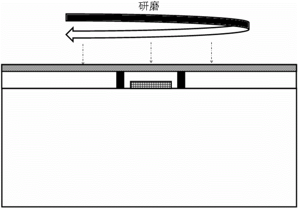
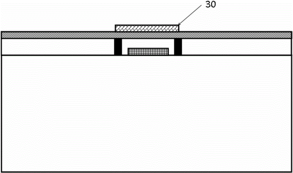
[0040] Figure 5 , Image 6 , Figure 7 , Figure 8 , Figure 9 and Figure 10 Each step of the method for preparing a transmission electron microscope sample according to a preferred embodiment of the present invention is schematically shown.

[0041] like Figure 5 , Image 6 , Figure 7 , Figure 8 , Figure 9 and Figure 10 As shown, the method for preparing a transmission electron microscope sample according to a preferred embodiment of the present invention includes:

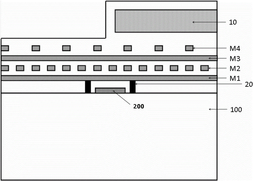
[0042] The first step: form a mark 300 for demarcating the specific target 200 for the specific target 200 on the sample that needs to be analyzed, such as Figure 5 as shown in the top view;

[0043] Wherein, in the first step S1, a laser or an ion beam can be ...


PUM

PropertyMeasurementUnit
thicknessaaaaaaaaaa

Abstract

The invention provides a method for preparing a transmission electron microscope sample. The method comprises the following steps: I, forming a marker for marking a specific target for the specific target to be analyzed on a sample; II, injecting a focused ion beam into a chip sample, finding an area of the specific target according to the marker, and cutting the chip sample till a position which is in a preset distance from the specific target by using an ion beam perpendicular to the sample; III, inclining the sample, cutting a target structure by using another ion beam in a preset inclined angle, observing a graph at the target by using an electron beam, judging, and cutting the part above the specific target till a position of a residual preset thickness; IV, inclining a sample plane to be perpendicular to the ion beam, and depositing a metal protection layer above the target structure; V, manufacturing the transmission electron microscope sample by using the metal protection layer, thereby forming the transmission electron microscope sample.

Description

technical field [0001] The present invention relates to the field of integrated circuit analysis, and more particularly, the present invention relates to a method for preparing transmission electron microscope samples. Background technique [0002] Transmission electron microscopy is widely and increasingly important in various fields including integrated circuit analysis, and double-beam focused ion beam (FIB) sample preparation is the most important method of transmission electron microscope sample preparation in the semiconductor field. [0003] Since the sample size of the TEM sample is very small, only on the micron level, in order to better control the thickness of the TEM sample, it is generally required that the surface of the chip sample is about 0.1 to 0.5 meters away from the analysis structure below it before the focused ion beam sample preparation begins. Microns. However, due to the different process steps of many chip samples, there are often thick multi-laye...

Claims


Application Information

Patent Timeline
Patent Type & Authority Applications(China)
IPC IPC(8): G01N1/28
CPCG01N1/286G01N2001/2873
Inventor 陈强孙蓓瑶
Owner SHANGHAI HUALI MICROELECTRONICS CORP
Why Eureka
Try Eureka