
Display panel and display device

A technology for display panels and substrate substrates, applied in the direction of planar/plate-shaped light guides, static indicators, instruments, etc., can solve problems such as quantum dot depolarization, thick liquid crystal cells, and damage to the polarization state of incident light, so as to improve the transmittance Overrate, avoid depolarization, improve the effect of response time

Active Publication Date: 2017-11-24
BOE TECH GRP CO LTD
View PDF6 Cites 8 Cited by
  • Summary
  • Abstract
  • Description
  • Claims
  • Application Information

AI Technical Summary

Problems solved by technology

[0003] In the prior art, the color color resistance in the color filter substrate can be made of quantum dot material, and the use of quantum dot material as the color color resistance can improve the color gamut of the display panel, but the quantum dot material will destroy the polarization state of the incident light, thus Causes the problem of depolarization of quantum dots, so quantum dot materials cannot be applied to liquid crystal display devices
[0004] The use of polarizers in the display panels of liquid crystal display devices in the prior art will lead to very low transmittance of the liquid crystal display device (for example, the transmittance is about 7%) and the thickness of the liquid crystal cell is relatively large (for example, 3um-5um) , and a larger cell thickness will reduce the response time of the liquid crystal

Method used


Image

  • Display panel and display device
  • Display panel and display device
  • Display panel and display device

Examples


Embodiment Construction

[0040] In order for those skilled in the art to better understand the technical solution of the present invention, the display panel and the display device provided by the present invention will be described in detail below with reference to the accompanying drawings.

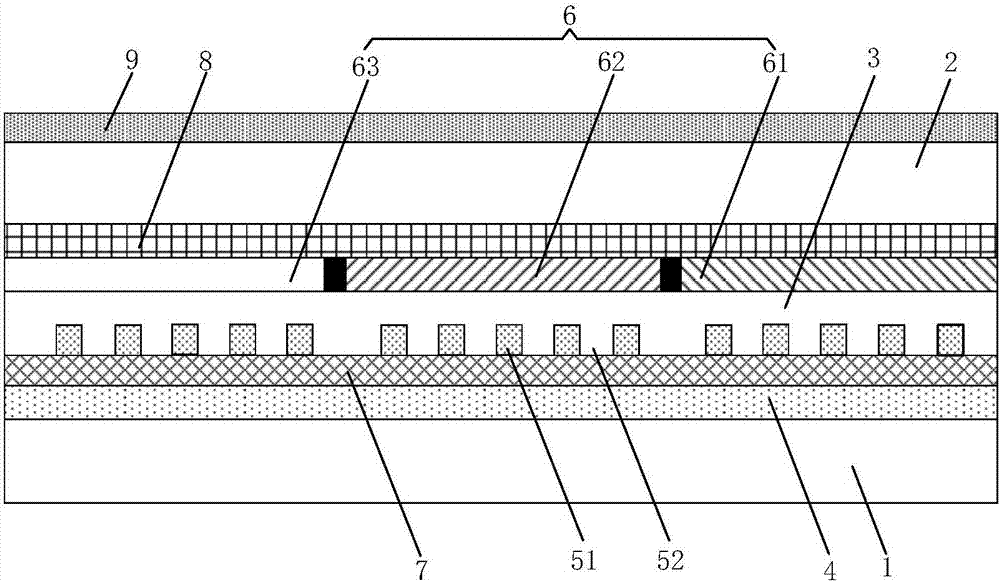
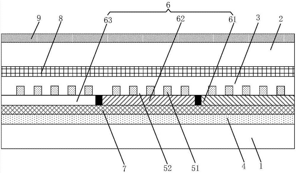
[0041] figure 1 A schematic structural diagram of a display panel provided in Embodiment 1 of the present invention, as shown in figure 1 As shown, the display panel includes: a first base substrate 2, a liquid crystal layer 3, a waveguide layer 4, a grating layer, a quantum dot color filter layer 6, a first electrode 8 and a second electrode 7, a liquid crystal layer 3, a grating layer , the quantum dot color filter layer 6 , the first electrode 8 and the second electrode 7 are located between the waveguide layer 4 and the first base substrate 2 . The first electrode 8 and the second electrode 7 are used to adjust the refractive index of the liquid crystal layer 3; the grating layer is used to control the cou...


PUM

PropertyMeasurementUnit
thicknessaaaaaaaaaa
thicknessaaaaaaaaaa
thicknessaaaaaaaaaa

Abstract

The invention discloses a display panel and a display device. The display panel includes: including: a first base substrate, a liquid crystal layer, a waveguide layer, a grating layer, a quantum dot color filter layer, a first electrode and a second electrode, and the first electrode and the second electrode are used for Adjusting the refractive index of the liquid crystal layer; the grating layer is used to control light coupling out of the waveguide layer, and the coupling efficiency of the waveguide layer for coupling out light depends on the refractive index of the liquid crystal layer and the refractive index of the grating layer The difference is determined. In the present invention, there is no need to set polarizers in the display panel, which avoids the problem of depolarization of quantum dots, so that quantum dot materials can be applied to liquid crystal display devices; the transmittance of the display panel is improved; and the thickness of the liquid crystal box can be set The thinner, which improves the response time of the liquid crystal.

Description

technical field [0001] The present invention relates to the field of display technology, in particular to a display panel and a display device. Background technique [0002] In the field of display technology, a liquid crystal display device includes a backlight source and a display panel. The display panel includes an array substrate and a color filter substrate oppositely arranged. A liquid crystal layer is arranged between the array substrate and the color filter substrate. Polarizers are arranged on the back side. The deflection of liquid crystal is controlled by voltage and controlled by two layers of polarizers to achieve gray scale display. [0003] In the prior art, the color resistance in the color filter substrate can be made of quantum dot material, and the use of quantum dot material as the color resistance can improve the color gamut of the display panel, but the quantum dot material will destroy the polarization state of the incident light, thus The problem o...

Claims


Application Information

Patent Timeline
Patent Type & Authority Patents(China)
IPC IPC(8): G02F1/1335
CPCG02F1/133504G02F1/133514G02F1/133615G02F1/133617G02F2202/36G02B6/005G02F1/133614G02F1/1326G02F1/136G09G3/36
Inventor 谭纪风王维董学
Owner BOE TECH GRP CO LTD
Learn More