Memory and method of forming the same

A memory and substrate technology, applied in semiconductor devices, electrical solid state devices, electrical components, etc., can solve the problems affecting the production yield of memory, control gate and substrate leakage, etc., and achieve the effect of improving production rate and avoiding leakage.

Active Publication Date: 2019-07-02
SEMICON MFG INT (SHANGHAI) CORP
View PDF3 Cites 0 Cited by
  • Summary
  • Abstract
  • Description
  • Claims
  • Application Information

AI Technical Summary

Problems solved by technology

[0004] However, after the memory in the prior art is formed, leakage between the control gate and the substrate is prone to occur, which will affect the production yield of the memory to a certain extent.

Method used


Image

  • Memory and method of forming the same
  • Memory and method of forming the same
  • Memory and method of forming the same

Examples


Embodiment Construction

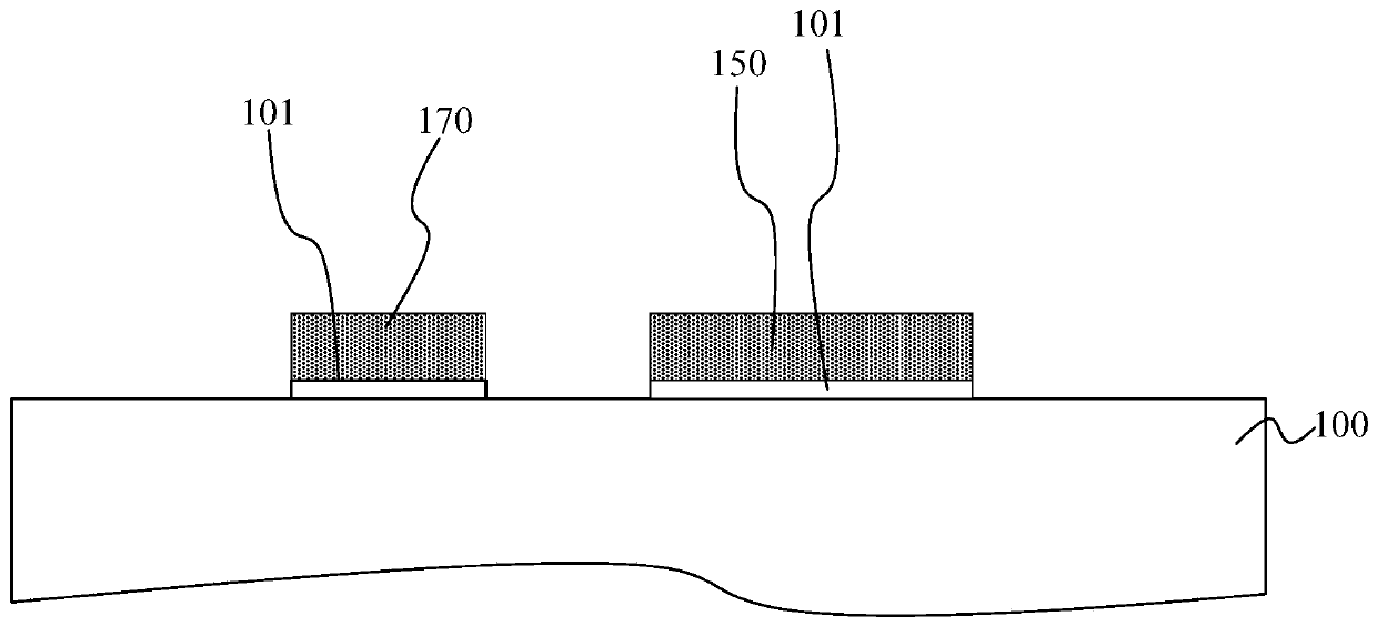
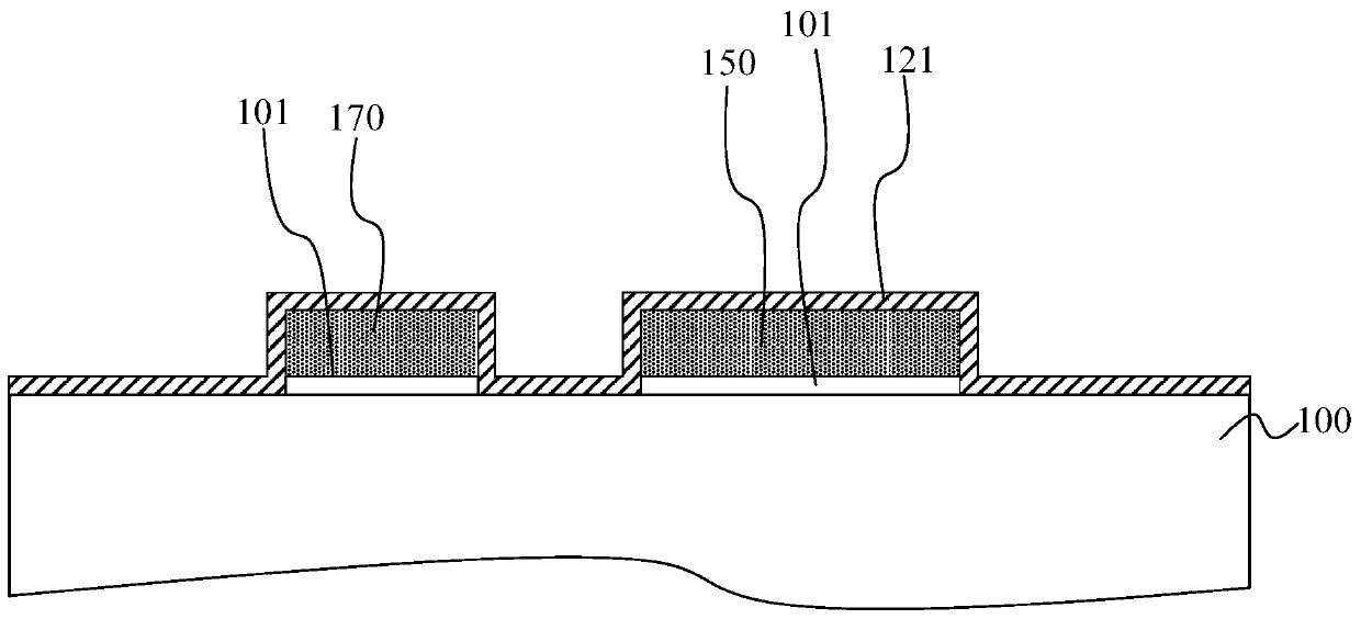
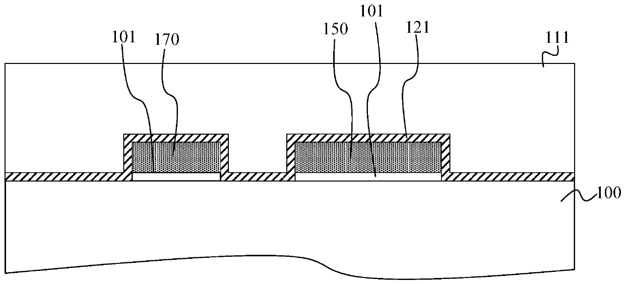
[0044] After the memory in the prior art is formed, electric leakage between the control gate and the substrate is prone to occur, which will affect the production yield of the memory to a certain extent. The specific reasons are as follows:

[0045] Taking an electrically erasable programmable read-only memory (EEPROM) as an example, in the process of forming this kind of memory, it is necessary to form a floating gate on the substrate, and then, on the floating gate and the substrate The material layer of the sidewall and the material layer of the control gate are formed at one time. After that, it is necessary to etch the material layer of the control gate to form the control gate, and then etch the exposed material layer of the sidewall to form the sidewall. However, it is difficult to ensure that the sidewalls of the sidewalls formed by etching in the prior art are absolutely flat, and the sidewalls of the sidewalls are easily uneven to form undercuts. The problem of ch...


PUM


Abstract

The invention provides a memory and its forming method. The forming method of the memory includes providing a substrate; forming a side wall material layer; forming a control gate material layer; etching the control gate material layer to form a control gate; the etched part is located on the substrate The side wall material layer is used to form a side wall layer; the side wall layer has a gap at the edge of the part of the substrate; an insulating filling layer is formed to fill the gap. The memory includes a substrate; a floating gate; a control gate located on the floating gate and a part of the substrate around the floating gate; a sidewall layer located between the floating gate and the control gate, and between the substrate and the control gate; the sidewall layer There is a notch at the edge of the portion located on the substrate; an insulating filling layer filling the notch of the sidewall layer. The beneficial effect of the present invention is that an insulating filling layer is formed at the gap of the side wall layer, and the insulating filling layer can fill the gap, thereby reducing the probability of charge leakage, thereby improving the production rate of the memory.

Description

technical field [0001] The invention relates to the field of semiconductors, in particular to a memory and a forming method thereof. Background technique [0002] In the prior art, various types of memory are widely used, among which non-volatile memory, such as erasable programmable read-only memory (electrically programmable read-only memory, EPROM), electrically erasable programmable read-only memory (EPROM) Electrically-erasable programmable read-only memory (EEPROM) and flash memory (flash memory) are currently widely used as data storage devices in computer systems, etc., and have received extensive attention. [0003] Among them, EEPROM can perform "one storage unit, one storage unit" (Byte By Byte) when clearing and re-inputting data, and data can be stored, read, and cleared multiple times. [0004] However, after the memory in the prior art is formed, electric leakage between the control gate and the substrate is prone to occur, which will affect the production yi...

Claims


Application Information

Patent Timeline
Patent Type & Authority Patents(China)
IPC IPC(8): H01L27/11521
CPCH10B41/30
Inventor 代洪刚李俊
Owner SEMICON MFG INT (SHANGHAI) CORP
Why Eureka
Try Eureka