Band engineered high-K tunnel oxides for non-volatile memory

a technology of non-volatile memory and tunnel oxides, which is applied in the direction of transistors, electrical devices, semiconductor devices, etc., can solve the problems of slow data writing into such memories, and inability to meet the requirements of microseconds, so as to improve programming speed and data retention, reduce charge leakage, and accelerate programming speed

Inactive Publication Date: 2011-01-25
SEAGATE TECH LLC
View PDF9 Cites 0 Cited by
  • Summary
  • Abstract
  • Description
  • Claims
  • Application Information

AI Technical Summary

Benefits of technology

[0003]The present disclosure relates to crested barriers composed of band engineered high-K dielectric materials that improve the programming speed and data retention (e.g., reduce charge leakage) for non-volatile memory, e.g., flash memory. Multiple layers of high-K dielectric materials are selected to form a digitally crested tunnel barrier. Alternately, compositionally graded materials are used to form the digitally crested tunnel barrier. The crested tunnel barriers have a potential energy profile that peaks between the charge supply region and the charge storage region and that decreases from the peak to the charge supply region and to the charge storage region. Such a barrier allows faster programming speed and longer retention time, as compared to a flat-band tunnel barrier conventionally implemented in non-volatile memory, e.g., flash memory. Also disclosed are storage devices utilizing the crested tunnel barriers.

Problems solved by technology

Non-volatile memories can store data without power supply for long periods of time, such as a year or more, but the act of writing data into such memories is slow, requiring microseconds.
Parabolic barriers and stepped barriers have been proposed, but suitable and practical configurations and methods of making the barriers have been lacking.

Method used


Image

  • Band engineered high-K tunnel oxides for non-volatile memory
  • Band engineered high-K tunnel oxides for non-volatile memory
  • Band engineered high-K tunnel oxides for non-volatile memory

Examples


first embodiment

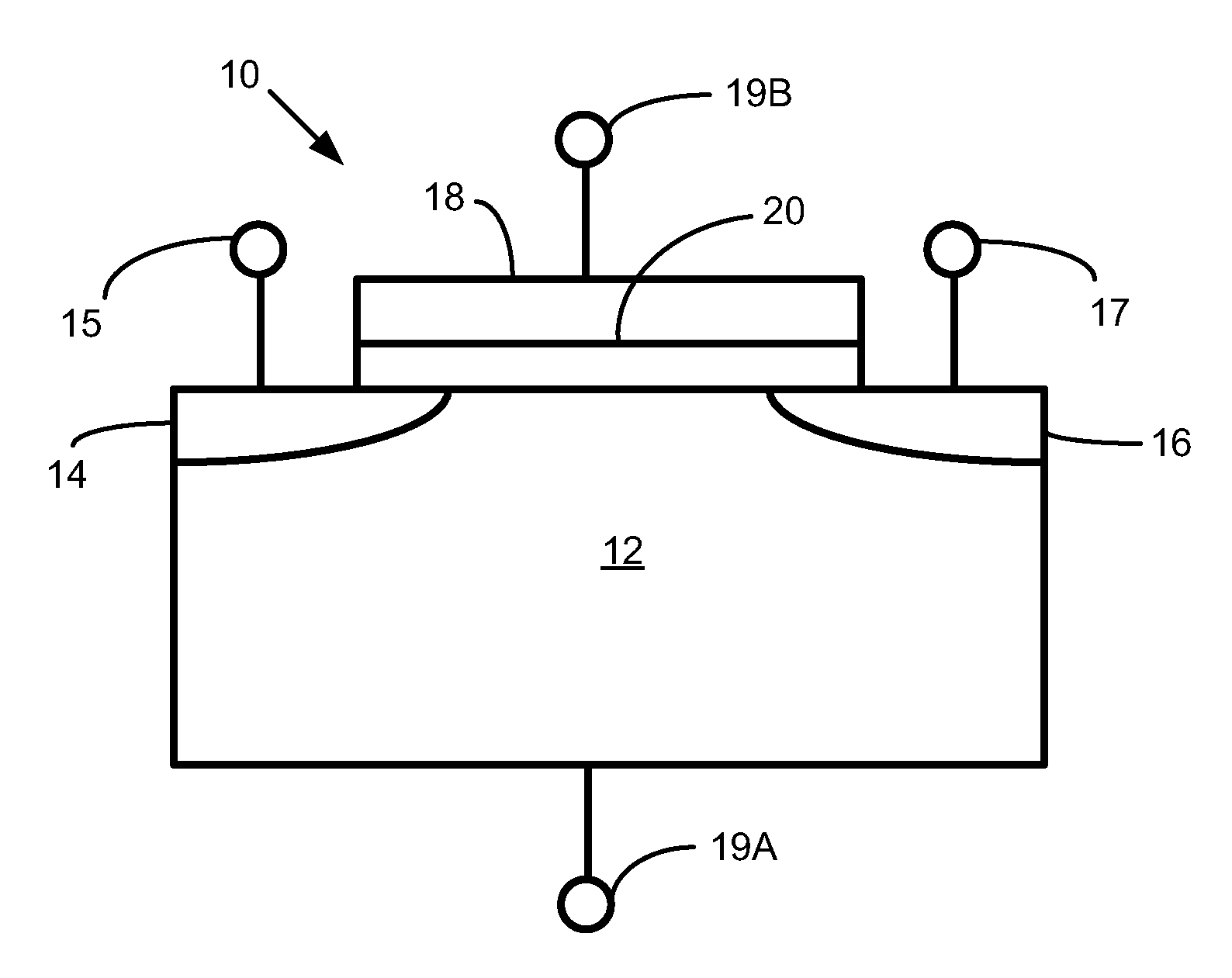
[0025]A first embodiment for a band engineered crested tunnel barrier is illustrated in FIGS. 5 and 6. FIG. 5 shows a tunnel barrier 50 having a plurality of individual layers 52, arranged as an inner region 54 and outer regions 56, 58. In the illustrated embodiment, tunnel barrier 50 has nine layers 52. Inner region 54 includes at least one of those layers 52 and each of outer regions 56, 58 include at least one of those layers 52. Band engineered crested tunnel barriers in accordance with this disclosure have at least three individual layers, usually at least five individual layers. In most embodiments, the number of layers is an odd number, so that a central layer has an equal number of layers on each side thereof. Other examples of band engineered crested tunnel barriers may have seven, eleven, thirteen, fifteen, etc. individual layers. The thickness of barrier layer 50 is often less than about 200 Angstroms, in some embodiments less than about 100 Angstroms. The thickness of ea...

second embodiment

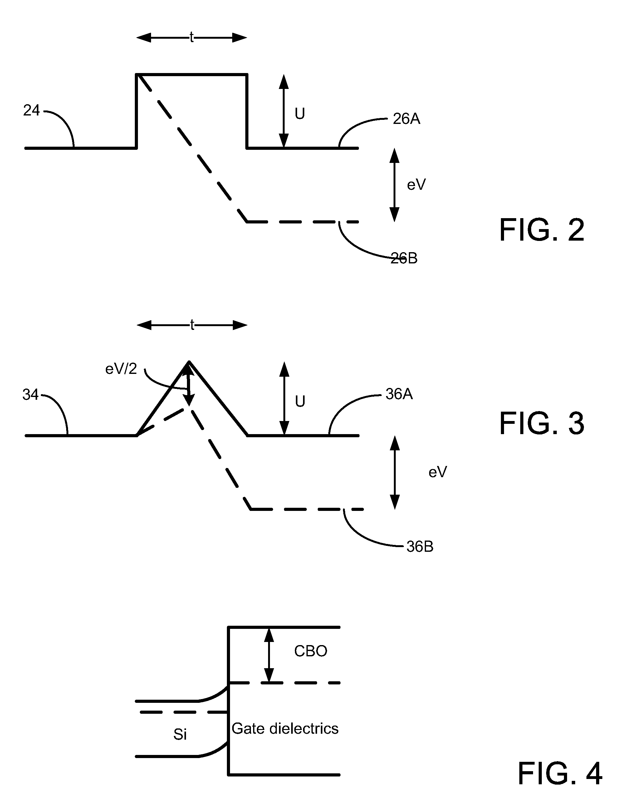
[0034]This second embodiment crested tunnel barrier is formed from a single layer of material that is compositionally graded across its thickness. Two or more high-K dielectric materials are combined to create the crested energy profile having an inner region and two outer regions. In this embodiment, the mole fraction of the high-K materials varies from the inner region to the outer regions and across the thickness of the layer. FIG. 7 illustrates a crested energy profile 70 having an inner region 74 having a higher potential energy profile than outer regions 76, 78. For outer regions 76, 78 of the tunnel barrier layer, those proximate the charge supply or source region and the storage region, the material is predominately the high-K material having the lower CBO. Inner region 74 at the center of the tunnel barrier layer, the material is predominantly the high-K material having the highest CBO.

[0035]To obtain the energy barrier illustrated in FIG. 7, two high-K dielectric materials...


PUM


Abstract

A non-volatile memory cell that has a charge source region, a charge storage region, and a crested tunnel barrier layer that has a potential energy profile which peaks between the charge source region and the charge storage region. The tunnel barrier layer has multiple high-K dielectric materials, either as individual layers or as compositionally graded materials.

Description

BACKGROUND[0001]Semiconductor memory devices are used in various electronic devices. For example, non-volatile semiconductor memory is used in cellular telephones, digital cameras, personal digital assistants, mobile computing devices, non-mobile computing devices and other devices. Electrical Erasable Programmable Read Only Memory (EEPROM) and flash memory are among the most popular non-volatile semiconductor memories. Non-volatile memories can store data without power supply for long periods of time, such as a year or more, but the act of writing data into such memories is slow, requiring microseconds.[0002]Attempts have been made to enhance memory performance, by using “crested” barriers, with the potential barrier height peaking in the middle and decreasing toward the interfaces with the electrodes. Parabolic barriers and stepped barriers have been proposed, but suitable and practical configurations and methods of making the barriers have been lacking.BRIEF SUMMARY[0003]The pres...

Claims


Application Information

Patent Timeline
Patent Type & Authority Patents(United States)
IPC IPC(8): H01L29/788
CPCH01L29/792
Inventor TIAN, WEIJIN, INSIKDIMITROV, DIMITAR V.XUE, SONG S.
Owner SEAGATE TECH LLC
Why Eureka
Try Eureka