
Three-dimensional nonvolatile semiconductor memory based on nanocrystalline floating gate and preparation method thereof

A non-volatile, nano-crystalline technology, applied in semiconductor devices, electrical solid-state devices, electrical components, etc., can solve the problem of long-term stable storage demand contradictions, weak shrinking properties of nano-crystalline metals, and limited space for increasing storage capacity. Achieve good data retention characteristics, increase the number of stacked layers, and reduce the effect of charge leakage

Active Publication Date: 2019-08-16
HUAZHONG UNIV OF SCI & TECH
View PDF5 Cites 0 Cited by
  • Summary
  • Abstract
  • Description
  • Claims
  • Application Information

AI Technical Summary

Problems solved by technology

[0003] However, in the three-dimensional flash memory structure, due to the limitation of the gate structure, there is a serious contradiction between the requirements of fast write / erase operations and the requirements of long-term stable storage.
And with the continuous increase of the number of three-dimensional stacking layers and the continuous reduction of the feature size, this contradiction is more significant
On the other hand, in the three-dimensional structure, the crosstalk of the floating gate structure is also very serious
[0004] In recent years, although it has been reported that nanocrystalline metals are used as floating gate materials to realize multi-valued storage and increase the storage capacity of memory, nanocrystalline metals have weak proportional reduction characteristics, and the carrier concentration decreases significantly with size reduction. Increase storage capacity space is very limited

Method used

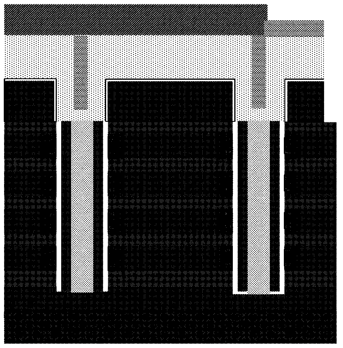
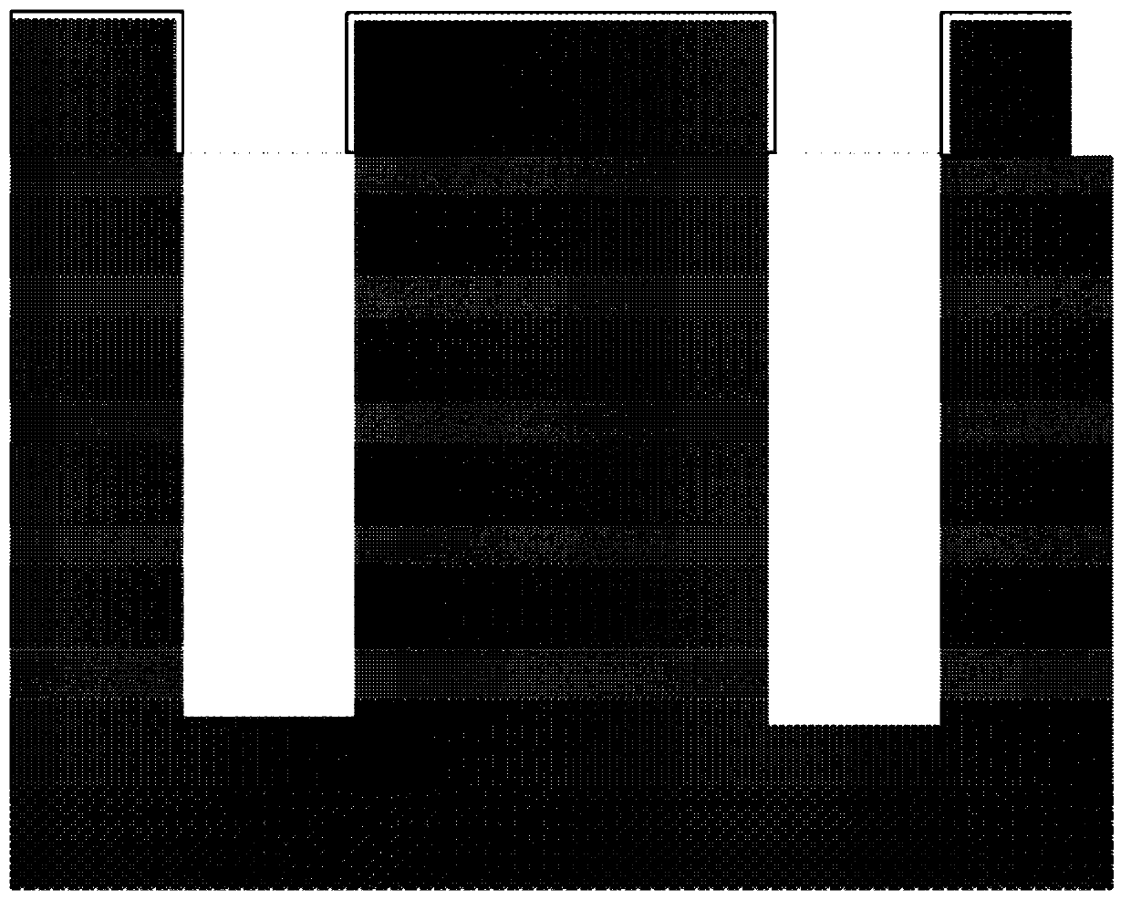
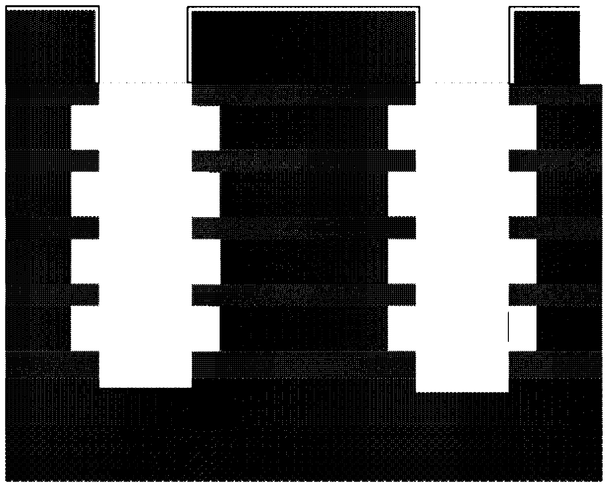

Image

  • Three-dimensional nonvolatile semiconductor memory based on nanocrystalline floating gate and preparation method thereof
  • Three-dimensional nonvolatile semiconductor memory based on nanocrystalline floating gate and preparation method thereof
  • Three-dimensional nonvolatile semiconductor memory based on nanocrystalline floating gate and preparation method thereof

Examples


Embodiment Construction

[0030] In order to make the object, technical solution and advantages of the present invention clearer, the present invention will be further described in detail below in conjunction with the accompanying drawings and embodiments. It should be understood that the specific embodiments described here are only used to explain the present invention, not to limit the present invention. In addition, the technical features involved in the various embodiments of the present invention described below can be combined with each other as long as they do not constitute a conflict with each other.

[0031] Aiming at the defects of the prior art, the present invention provides a non-volatile three-dimensional semiconductor memory based on nanocrystalline floating gate, which includes a plurality of three-dimensional NAND memory strings in the vertical direction, and one memory cell can store at least 2 bits of data.

[0032] By changing the type of floating gate material and the correspondin...


PUM


Abstract

The invention belongs to the field of three-dimensional flash memory preparation, and more particularly to a three-dimensional nonvolatile semiconductor memory based on a nanocrystalline floating gateand a preparation method thereof. The three-dimensional semiconductor memory includes a plurality of three-dimensional NAND memory strings in a vertical direction, wherein each three-dimensional NANDmemory string includes a semiconductor region, and a four-layered package structure surrounding the semiconductor region and including a tunneling dielectric layer, a charge storage layer, a barrierdielectric layer and a control gate electrode; the material of the charge storage layer comprises a nanocrystalline material; and the nanocrystalline material is a sulfur-based compound nanocrystalline. The sulfur-based compound nanocrystalline having a high hole structure content is used as the material of the charge storage layer, thereby improving the programming / erasing efficiency, the programming / erasing speed, and the charge storage capability of a single memory cell of the three-dimensional flash memory. The process of the nanocrystalline floating gate of the invention is simple and iscompatible with a vertical channel process.

Description

technical field [0001] The invention belongs to the field of preparation of a three-dimensional flash memory, and more specifically relates to a three-dimensional nonvolatile semiconductor memory based on a nanocrystal floating gate and a preparation method thereof. Background technique [0002] The storage density of the three-dimensional flash memory is no longer limited by the feature size of the process, and the storage density can be continuously improved by stacking in the vertical direction. [0003] However, in the three-dimensional flash memory structure, due to the limitation of the gate structure, there is a serious contradiction between the requirement of fast write / erase operation and the requirement of long-term stable storage. And with the continuous increase of the number of three-dimensional stacked layers and the continuous reduction of the feature size, this contradiction becomes more significant. On the other hand, in the three-dimensional structure, the...

Claims


Application Information

Patent Timeline
Patent Type & Authority Applications(China)
IPC IPC(8): H01L27/11521H01L27/11556H10B41/30H10B41/27
CPCH10B41/27H10B41/30
Inventor 缪向水钱航童浩
Owner HUAZHONG UNIV OF SCI & TECH
Learn More