Inspection device and object inspection method

A technology for processed objects and inspection devices, applied in the fields of instruments, nonlinear optics, optics, etc., can solve the problems of reducing overall process productivity and reducing process efficiency, and achieve the effect of improving efficiency and productivity and improving inspection efficiency.

Active Publication Date: 2021-08-10
CHARM ENG CO LTD
View PDF7 Cites 0 Cited by
  • Summary
  • Abstract
  • Description
  • Claims
  • Application Information

AI Technical Summary

Problems solved by technology

[0004] In the prior art, various processes for inspecting defects of the substrate are not carried out in one device, but are carried out in different devices from each other, thereby reducing the process efficiency and thus the productivity of the overall process.

Method used


Image

  • Inspection device and object inspection method
  • Inspection device and object inspection method
  • Inspection device and object inspection method

Examples


Embodiment Construction

[0042] Hereinafter, preferred embodiments of the present invention will be described in detail with reference to the accompanying drawings. However, the present invention is not limited in the embodiments disclosed below, but can achieve various forms different from each other. Embodiments of the present invention are merely disclosed in the present invention, and is provided to inform the scope of the present invention to inform the invention of the skilled articles of the invention. To illustrate an embodiment of the invention, the drawing can be expanded or exaggerated, and the same symbols in the map are called the same elements.

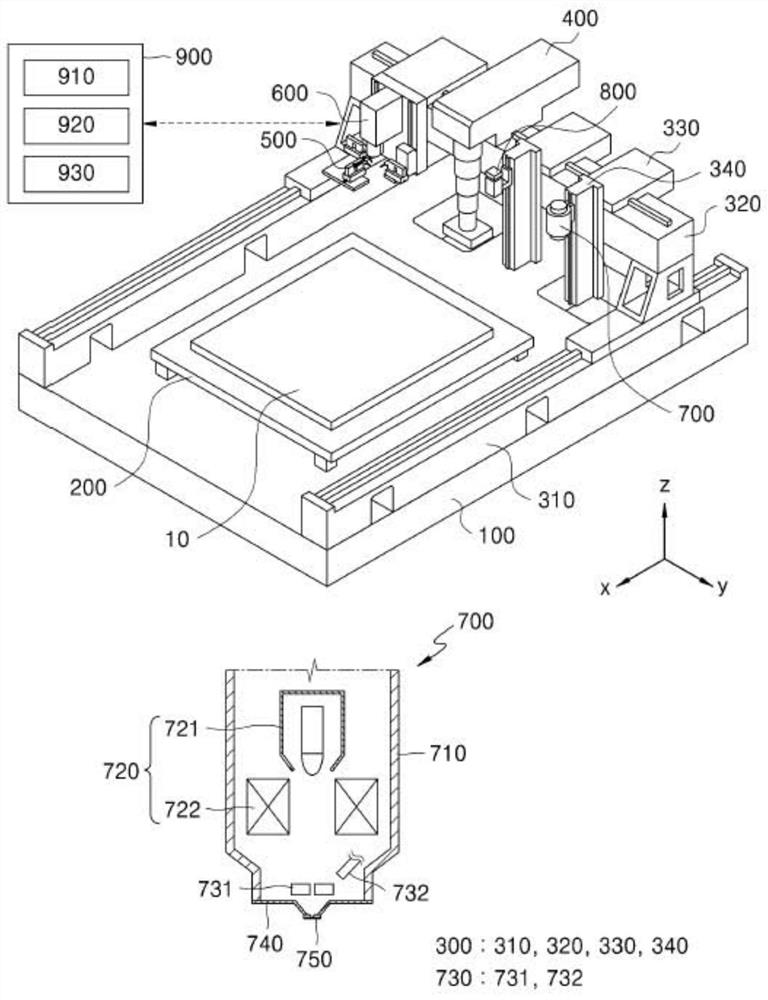
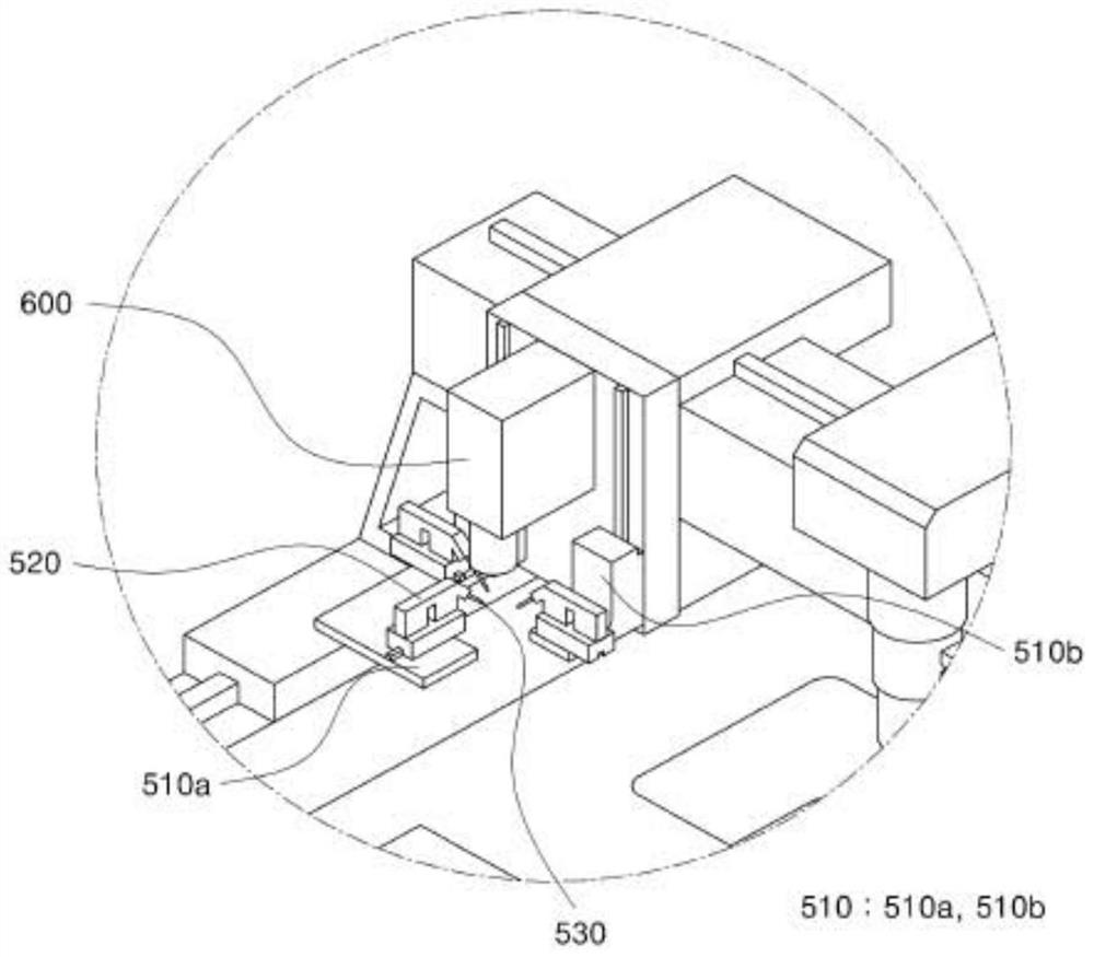
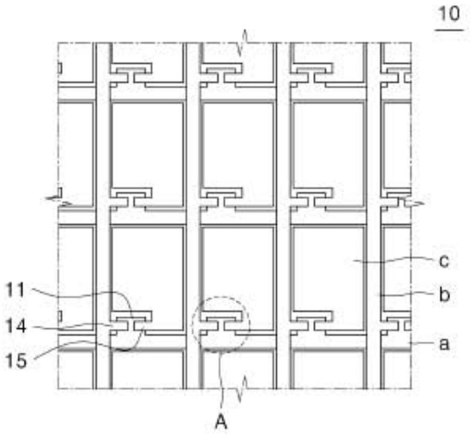
[0043] figure 1 It is a schematic view showing an inspection apparatus according to an embodiment of the present invention. figure 2 It is a portion of the inspection portion of the inspection apparatus according to an embodiment of the present invention. in addition, image 3 It is a schematic view showing the processed objects of the embodiment of...


PUM


Abstract

The present invention proposes an inspection device and a treatment object inspection method capable of inspecting defects of various objects to be processed with one device when inspecting defects of the object to be processed. The inspection device includes: a supporting part that supports the object to be processed; On the upper side of the support part, a part of the film formed on the upper part of the object to be processed is selectively removed by using a laser beam; the inspection part is arranged on the upper side of the support part and contacts the object to be processed an element to send and receive signals; an optical part disposed on the supporting part facing the inspection part so that the inspection part can be observed; and a control part using the image observed by the optical part to control the inspection movement of the department.

Description

Technical field [0001] The present invention relates to an inspection apparatus, more detailed, to the inspection apparatus capable of inspecting various defective defects, and a processed object inspection method capable of checking various defect defects when examining the defects of the treated product. Background technique [0002] A flat panel display device such as a Liquid Crystal Display (LCD) or OrganicLight Emitting Display, OLEDs, has a lower substrate that faces each other and an upper substrate, which fills a liquid crystal layer or an organic layer, or the like. A plurality of electrode gate lines and data lines are formed in the lower substrate and form a matrix structure, and a plurality of pixels are formed therefrom. For individual driving pixels, each pixel forms an action element (eg, a switching element) such as a switching element. [0003] Further, in the process of manufacturing a flat panel display device, when a different substance is attached to the pix...

Claims


Application Information

Patent Timeline
Patent Type & Authority Patents(China)
IPC IPC(8): G02F1/13
CPCG02F1/1309
Inventor 芮世熙
Owner CHARM ENG CO LTD
Why Eureka
Try Eureka