
Growth method for improving epitaxial yield of light emitting diode

A technology of light-emitting diodes and growth methods, which is applied in the growth field of improving the epitaxial yield of light-emitting diodes, and can solve problems affecting the yield of epitaxial wafers, poor consistency of epitaxial wafers, and amplification of differences, etc.

Active Publication Date: 2017-01-11
XIAMEN CHANGELIGHT CO LTD
View PDF3 Cites 1 Cited by
  • Summary
  • Abstract
  • Description
  • Claims
  • Application Information

AI Technical Summary

Problems solved by technology

[0006] The purpose of the present invention is to provide a growth method for improving the epitaxial yield of light-emitting diodes, to solve the problem that the influence of differences between PSS pattern substrates on the epitaxial growth process is amplified due to the inherent characteristics of AlN materials and PSS pattern substrates. During the epitaxial growth process, the consistency of the epitaxial wafers becomes poor, which affects the yield of the epitaxial wafers.

Method used


Image

  • Growth method for improving epitaxial yield of light emitting diode
  • Growth method for improving epitaxial yield of light emitting diode
  • Growth method for improving epitaxial yield of light emitting diode

Examples


Embodiment Construction

[0031] The present invention will be described in detail below in conjunction with the accompanying drawings and specific embodiments.

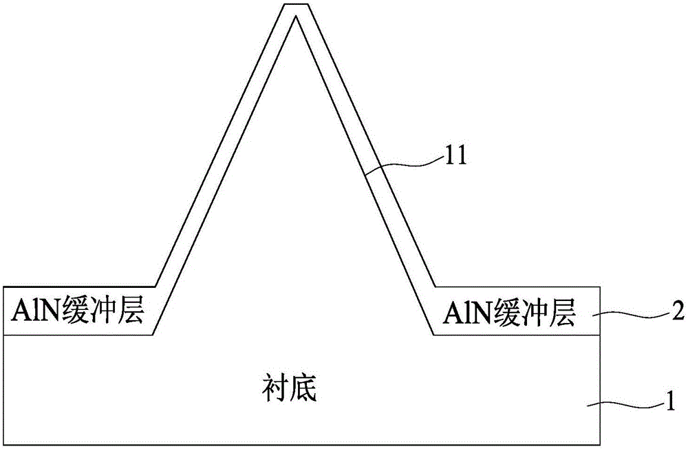
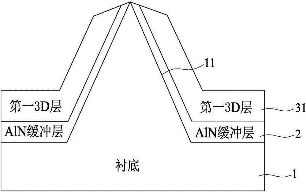
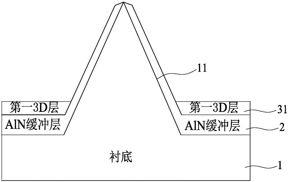
[0032] see Figure 1 to Figure 5 As mentioned above, a growth method for improving the epitaxy yield of light-emitting diodes disclosed in the present invention includes the following steps:

[0033] One, form a PSS pattern 11 on the substrate 1, adopt PVD to vapor-deposit the substrate 1, and form an AlN buffer layer 2 on the substrate 1, such as figure 1 shown. The thickness of the AlN buffer layer is less than 100nm. If the thickness of the AlN material is too thick, the etching cycle of MOCVD will become more, which will increase the cost and growth time, making the technology of PVD vapor deposition of AlN lose its advantages.

[0034] Second, MOCVD is used to three-dimensionally grow the first 3D layer 31 on the AlN buffer layer, and the first 3D layer 31 is GaN, such as figure 2 shown. Due to growth characteristics, the thickness...


PUM

PropertyMeasurementUnit
Thicknessaaaaaaaaaa

Abstract

The invention discloses a growth method for improving the epitaxial yield of a light emitting diode. The method includes steps: firstly, performing evaporation deposition on a substrate by employing PVD; secondly, growing a first 3D layer on an AlN buffer layer in a three-dimensional manner by employing MOCVD; thirdly, etching the first 3D layer on side surfaces of a PSS pattern and on the plane of the substrate until the first 3D layer on the side surfaces of the PSS pattern are completely etched; fourthly, performing cooling, and continuously growing a second 3D layer in a three-dimensional manner; fifthly, etching the second 3D layer on the side surfaces of the PSS pattern and on the plane of the substrate until the second 3D layer on the side surfaces of the PSS pattern are completely etched, wherein the AlN buffer layer on the side surfaces of the PSS pattern is partly etched, and the second 3D layer on the plane is partly etched; sixthly, repeating the above steps for multiple times in a circulating manner; and seventhly, growing an unintentionally-doping layer, an n-type conducting layer, an active region, and a P-type conducting layer in sequence on the 3D layer at the top. According to the method, the problem that the consistency of epitaxial wafers becomes poorer in an epitaxial growth process so that the yield of the epitaxial wafers is influenced is solved.

Description

technical field [0001] The invention relates to the technical field of light-emitting diodes, in particular to a growth method for improving the epitaxy yield of light-emitting diodes. Background technique [0002] In recent years, the rapid development of light-emitting diodes is closely related to the development of semiconductor optoelectronic technology and new lighting source technology. With the continuous expansion of LED application fields, the improvement of LED chip brightness and cost reduction have become the focus of current development. [0003] In the prior art, the use of PVD equipment to vapor-deposit AlN substrates, as an effective way to reduce costs and increase yields, is gradually being accepted and becoming a mainstream technology. However, the use of PVD to evaporate AlN substrates currently has problems such as repeatability and poor consistency of epitaxy process results. [0004] The traditional technology can effectively improve the large-scale ...

Claims


Application Information

Patent Timeline
IPC IPC(8): H01L33/00H01L33/12H01L21/203
CPCH01L21/0254H01L21/02631H01L33/005H01L33/12
Inventor 汪洋林志伟童吉楚程伟陈凯轩姜伟卓祥景王爱民
Owner XIAMEN CHANGELIGHT CO LTD
Learn More