AMOLED display manufacturing method and AMOLED display

A manufacturing method and display technology, which can be used in semiconductor/solid-state device manufacturing, electrical solid-state devices, semiconductor devices, etc., and can solve the problems of large limitations of AMOLED displays.

Active Publication Date: 2017-01-11
KUNSHAN NEW FLAT PANEL DISPLAY TECH CENT
View PDF4 Cites 6 Cited by
  • Summary
  • Abstract
  • Description
  • Claims
  • Application Information

AI Technical Summary

Problems solved by technology

However, on the basis of existing materials and process equipment...

Method used


Image

  • AMOLED display manufacturing method and AMOLED display
  • AMOLED display manufacturing method and AMOLED display
  • AMOLED display manufacturing method and AMOLED display

Examples


Embodiment 1

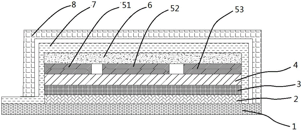
[0042] like figure 1 As shown, the structure of the AMOLED display provided by the method described in this application is the same as that of the existing AMOLED display, and the AMOLED display includes a second substrate 1, an AMOLED light-emitting area and an encapsulation layer 8, and the AMOLED light-emitting area is arranged on the second substrate 1, the encapsulation layer 8 is arranged on the top and around the AMOLED light-emitting area to encapsulate the AMOLED light-emitting area.

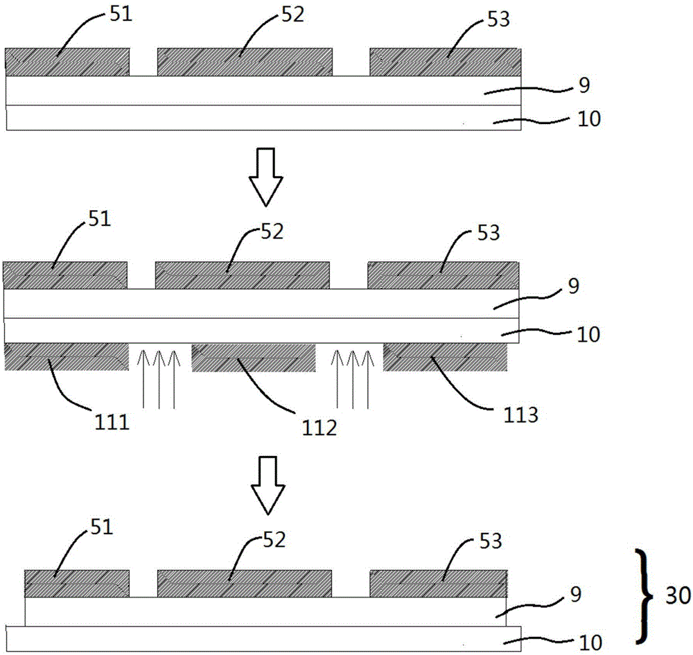
[0043] The AMOLED light-emitting area includes cathode 7, electron layer 6, light-emitting layers 51 / 52 / 53, hole layer 4, anode 3 and thin film transistor 2 (TFT) arranged in sequence from top to bottom. The thin film transistor 2 is attached to the second substrate 1 .

[0044] Wherein, the second substrate 1 is generally made of a transparent polymer material, such as polyimide (PI), as a substrate of an AMOLED display. The TFT 2 includes a gate, a gate insulating layer, an active l...


PUM

PropertyMeasurementUnit
Energy densityaaaaaaaaaa
Frequencyaaaaaaaaaa

Abstract

The invention relates to an AMOLED display manufacturing method and AMOLED display. Technically, the method comprises the following steps: preparing a phase change material layer and a light emitting layer on one side of a first substrate in sequence, followed by the covering and the laser processing of a mask pattern at the other side of the first substrate to obtain part A; preparing a film transistor, an anode and a hole layer on a second substrate in sequence to obtain part B; bonding the light emitting layer of part A and the hole layer of part B; and removing the first substrate and the phase change material layer, preparing in sequence an electron layer and a cathode at the position of the original phase change material layer, and then packaging for an AMOLED display. Through the use of a phase change material layer in the manufacturing process, it is possible to reduce the pixel pitch in the light emitting layer without changing other materials and steps to obtain an AMOLED display with a high PPI.

Description

technical field [0001] The present application relates to the field of flat panel display technology, and in particular, relates to a manufacturing method of an AMOLED display and a corresponding AMOLED display. Background technique [0002] Active-matrix organic light emitting diode (Active-matrix organic light emitting diode, AMOLED for short) display is called the next-generation display technology. Compared with existing liquid crystal displays such as mobile phones, TVs, and monitors, AMOLED displays have wider viewing angles, higher refresh rates, and thinner sizes. With the characteristics of wide color gamut and low working voltage, it is considered to be the most potential display device. [0003] The number of pixels (Pixels Per Inch, PPI for short) is a unit of image resolution, which represents the number of pixels (Pixels) per inch of the display. Therefore, the higher the PPI value, it means that the display screen can display images with higher density, and ...

Claims


Application Information

Patent Timeline
IPC IPC(8): H01L51/56H01L27/32
CPCH10K59/12H10K71/00
Inventor 丁立薇朱晖张小宝朱涛习王锋胡思明
Owner KUNSHAN NEW FLAT PANEL DISPLAY TECH CENT
Why Eureka
Try Eureka