A pixel structure and an organic light-emitting display using the pixel structure

A pixel structure and pixel technology, applied in the direction of semiconductor devices, electrical solid devices, electrical components, etc., can solve the problems that affect the improvement of the sub-pixel aperture ratio PPI, the improvement of the working brightness of monochrome devices, and the shortening of the life of the display screen, so that it is not easy to deform , increase the strength, reduce the effect of difficulty

Active Publication Date: 2017-06-20
KUNSHAN GO VISIONOX OPTO ELECTRONICS CO LTD +1
View PDF1 Cites 0 Cited by
  • Summary
  • Abstract
  • Description
  • Claims
  • Application Information

AI Technical Summary

Problems solved by technology

[0013] The result of the periodic arrangement of pixels is that the blue sub-pixels in the pixel array are arranged in a straight line, so that the corresponding metal mask must use the aforementioned slit or the aforementioned slot opening method, but as mentioned above, the slit and slot opening methods All have defects, which lead to the opening of the blue metal mask in the pixel array arrangement of IGNIS, which seriously affects the further improvement of the sub-pixel aperture ratio and PPI.
[0014] In addition, organic light-emitting display devices generally reduce the aperture ratio of sub-pixels as the resolution increases, resulting in increased operating brightness of monochrome devices and shortened display life.

Method used


Image

  • A pixel structure and an organic light-emitting display using the pixel structure
  • A pixel structure and an organic light-emitting display using the pixel structure
  • A pixel structure and an organic light-emitting display using the pixel structure

Examples


Embodiment 1

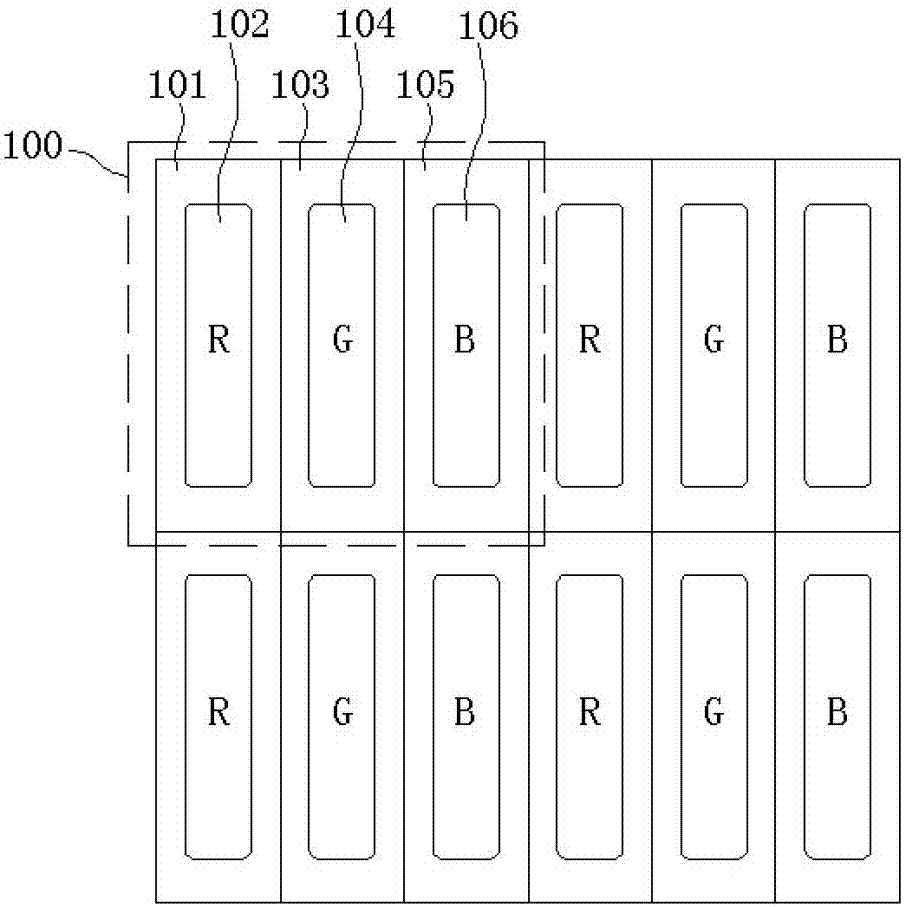
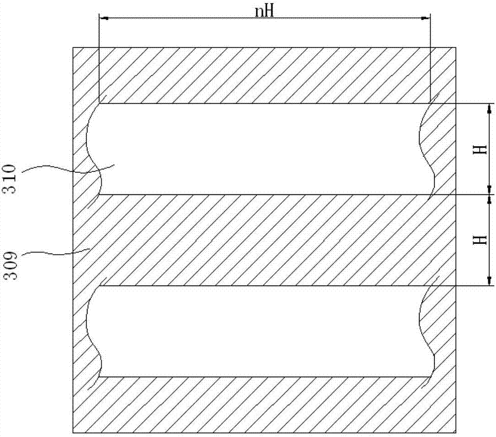
[0068] image 3 It is a schematic diagram of the first embodiment of the pixel structure of the organic light emitting display of the present invention. Such as image 3 As shown, the display includes a plurality of pixels 300, and each pixel 300 is composed of a plurality of sub-pixels. Each pixel 300 includes an R sub-pixel area 301 , an R light-emitting area 302 , a G sub-pixel area 303 , a G light-emitting area 304 , a B sub-pixel area 305 and a B light-emitting area 306 . The size of each pixel is H×H.

[0069] In this embodiment, the R, G, and B sub-pixels of each pixel are quadrangular, and the sub-pixels are arranged in the shape of a "pin" or an inverted "pin". Wherein, the length and width of the R and G sub-pixels are both 1 / 2H, and the width of the B sub-pixel is H, and the height is 1 / 2H, that is, the area of ​​the B sub-pixel is twice that of the G sub-pixel or the R sub-pixel.

[0070] Wherein, each pixel unit in this embodiment may be composed of an odd num...

Embodiment 2

[0081] Such as Figure 5 A second embodiment of the invention is shown. In this embodiment, the display includes a plurality of pixels 500, and each pixel is composed of a plurality of sub-pixels. The shape of each sub-pixel is a triangle. Preferably, as Figure 5 As shown, each sub-pixel is an isosceles right-angled triangle, and the right angles of every four sub-pixels are arranged opposite to each other to form a pixel. Four sub-pixels constituting one pixel include one R sub-pixel 501 , one G sub-pixel 503 and two B sub-pixels 502 , wherein the two B sub-pixels 502 are arranged opposite to each other. In this way, the area of ​​the B sub-pixel 502 is also twice that of the R sub-pixel 501 or the G sub-pixel 503, thereby ensuring the display effect of the display.

[0082] Such as Figure 5 As shown, this figure only shows a part of the organic light emitting display, and the number of pixels in the actual product is not limited to this. The first row, the second row...

Embodiment 3

[0093] For Example 2, we can replace some of the color sub-pixels with other colors, such as Image 6 In the third embodiment of the present invention shown, each pixel 600 in this embodiment is composed of an R sub-pixel 601 , a G sub-pixel 603 , a B sub-pixel 602 and a W (white) sub-pixel 604 . This example is compatible with Figure 5 Compared with the illustrated embodiment, one of the B sub-pixels is replaced by a W sub-pixel 604, and the positions of the R sub-pixel and the G sub-pixel are exchanged. The advantage of this embodiment is that since each pixel includes a W sub-pixel, it can display white more purely and achieve higher brightness.

[0094] Specifically, such as Image 6 As shown, the display includes a plurality of pixels 600, and each pixel is composed of a plurality of sub-pixels. The shape of each sub-pixel is a triangle. Preferably, as Image 6 As shown, each sub-pixel is an isosceles right-angled triangle, and the right angles of every four sub-pix...


PUM


Abstract

The invention discloses a pixel structure and an organic light-emitting display adopting the pixel structure. Wherein, the pixel structure includes a plurality of pixels, each pixel is composed of a plurality of sub-pixels, and at least one pixel constitutes a pixel unit. The present invention can increase the opening area of ​​the Mask during evaporation, reduce the difficulty of making the Mask process, and also reduce the evaporation process by using a reasonable pixel arrangement structure and sharing an opening on the Mask with the sub-pixels of adjacent pixels for evaporation. difficulty. There is no need to reserve a gap when evaporating the sub-pixels of the adjacent pixels of the Mask, and a real high PPI can be achieved while maintaining the requirements of the aperture ratio. In addition, the present invention can also increase the strength of the Mask, making it difficult to deform during use, improving product yield, extending the life of the Mask, and reducing costs.

Description

[0001] This application is a divisional application of an invention patent application with the application number 201310747572.1, the application date is December 31, 2013, and the title is "a pixel structure and an organic light-emitting display using the pixel structure". technical field [0002] The present invention relates to the field of organic light-emitting display technology, in particular to a pixel structure and an organic light-emitting display using the pixel structure. Background technique [0003] OLED (Organic Light-Emitting Diode, organic light-emitting diode) is an active light-emitting device. Compared with the traditional LCD (Liquid Crystal Display, liquid crystal display) display method, OLED display technology does not require a backlight and has the characteristic of self-luminescence. OLEDs use very thin layers of organic materials and glass substrates that emit light when an electric current passes through them. Therefore, OLED displays can signi...

Claims


Application Information

Patent Timeline
Patent Type & Authority Patents(China)
IPC IPC(8): H01L27/32
Inventor 张伸福邱勇彭兆基
Owner KUNSHAN GO VISIONOX OPTO ELECTRONICS CO LTD
Why Eureka
Try Eureka