
Four-station detection and cutting device for chip resistors

A cutting device and detection device technology, which is applied in the direction of manufacturing tools, metal processing equipment, optical testing flaws/defects, etc., can solve the problem of insufficient appearance accuracy of the inspected chip resistance, affecting the quality and function of the finished product, unstable quality of the chip resistance, etc. problems, to achieve low daily maintenance costs, reduce eye fatigue, and low power consumption

Inactive Publication Date: 2017-01-25
昆山市和博电子科技有限公司
View PDF7 Cites 4 Cited by
  • Summary
  • Abstract
  • Description
  • Claims
  • Application Information

AI Technical Summary

Problems solved by technology

[0002] The electronic market is developing rapidly, and the development of electronic passive components such as chip resistors has become high-quality and miniaturized. In the process of chip resistor inspection and cutting, the traditional manual inspection of the appearance and defects of chip resistors with the naked eye through a microscope, but artificial There are many shortcomings in the inspection. On the one hand, human eyes will be fatigued after long-term observation, which will lead to unstable chip resistor quality, low production efficiency, and insufficient appearance accuracy of the inspected chip resistor; on the other hand, it will lead to more product waste. If a bad product is detected in the chip resistor, it will be discarded together with the whole column of the chip resistor.
The appearance and defect detection of chip resistors are very critical in the entire manufacturing process. If the defect detection cannot be guaranteed, it will directly affect the quality and function of the finished product

Method used


Image

  • Four-station detection and cutting device for chip resistors

Examples


Embodiment Construction

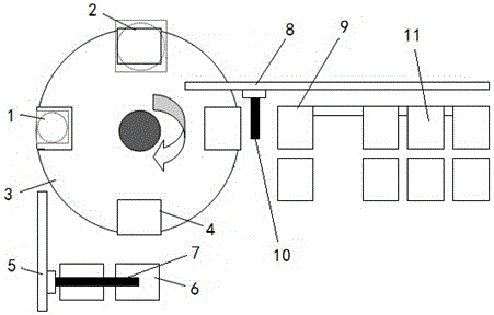
[0012] Attached below figure 1 The present invention will be further explained. Attached figure 1 It schematically shows the four-station detection and cutting device for chip resistors of the present invention, including an automatic control device, a feeding device, a detection device 1, a cutting device 2 and a receiving device, and is characterized in that it also includes a rotatable four-station The four-station disk 3 is uniformly fixed on the edge of the four-station disk 3 with four positioning clamps 4, and the four positioning clamps 4 are sequentially provided with matching feeding devices, detection devices 1, cutting devices 2, and receiving devices. The inspection device 1 is equipped with an industrial inspection camera, and the cutting device 2 is equipped with a laser.

[0013] Preferably, the four positioning fixtures 4 are provided with sensors.

[0014] Preferably, the feeding device includes a feeding guide rail 5 and a double feeding bin 6. A slidable feed...


PUM


Abstract

The invention discloses an efficient and automatic four-station detection and cutting device for chip resistors. The four-station detection and cutting device comprises an automatic control device, a feeding device, a detection device, a cutting device and a collecting device, and further comprises a four-station disc capable of rotating. Four positioning fixtures are evenly and fixedly arranged at the edge of the four-station disc, the feeding device, the detection device, the cutting device and the collecting device are sequentially arranged around the four positioning fixtures in cooperation, the detection device is provided with an industrial detection camera, and the cutting device is provided with a laser machine. By means of the four-station detection and cutting device, undesirable defects can be accurately and efficiently detected, and defective products can be removed in automatic laser cutting; through the four-station disc design, the automation degree is high, and the production efficiency is high; software can automatically generate product quality reports and production records according to the actual product detection condition; the four-station detection and cutting device achieves energy conservation and environmental protection, is low in power consumption and daily maintenance cost and reduces cost.

Description

Technical field [0001] The invention belongs to a detection device, and particularly relates to a wafer resistance detection and cutting device. Background technique [0002] The electronic market is developing rapidly. Electronic passive components such as chip resistors have developed into high-quality and miniaturized. In the chip resistor inspection and cutting process, the traditional manual microscope is used to detect the appearance and defects of chip resistors through the naked eye. There are many shortcomings in testing. On the one hand, human eyes will fatigue after long-term observation, which leads to unstable chip resistor quality, low production efficiency, and insufficient appearance accuracy of the chip resistor to be tested; on the other hand, it leads to more product waste. If a defective product is detected in the chip resistor, it will be discarded along with the entire row of the current chip. The appearance and defect detection of chip resistors are critic...

Claims


Application Information

Patent Timeline
IPC IPC(8): B23K26/38B23K26/70G01N21/88
CPCB23K26/38G01N21/88
Inventor 李刚何志峰
Owner 昆山市和博电子科技有限公司
Learn More