A test method and chip
A test method and chip technology, which is applied in the electronic field, can solve the problems of limited number of chips and affect test efficiency, and achieve the effect of reducing the number of probes, reducing interfaces, and improving test efficiency
- Summary
- Abstract
- Description
- Claims
- Application Information
AI Technical Summary
Problems solved by technology
Method used
Image

Examples
Embodiment 1
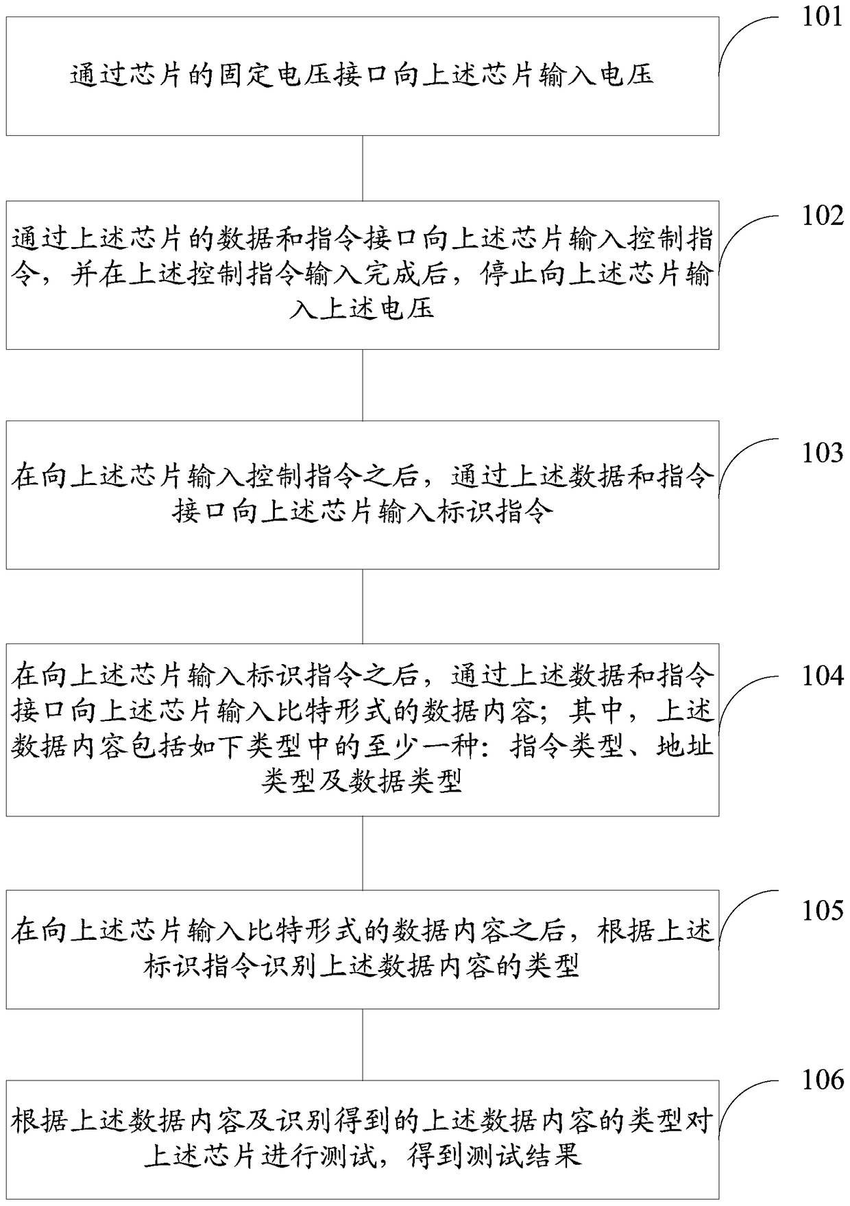
[0053] refer to figure 1 , which shows a flow chart of the steps of Embodiment 1 of a test method of the present invention, which may specifically include the following steps:
[0054] Step 101, inputting a voltage to the chip through a fixed voltage interface of the chip;
[0055] The embodiment of the present invention can be applied to wafer testing of chips. The wafer test is to test each die on the wafer to test some basic device parameters. A probe made of gold wire is installed on the detection head, and the contact PAD on the die Contact, test its electrical characteristics, the unqualified grains will be marked, and then when the wafer is cut into independent grains according to the grain, the marked unqualified grains will be eliminated, and no further processing will be carried out. A manufacturing process, so as not to increase the manufacturing cost.
[0056] In the embodiment of the present invention, the above-mentioned voltage is used to drive the chip to en...
Embodiment 2
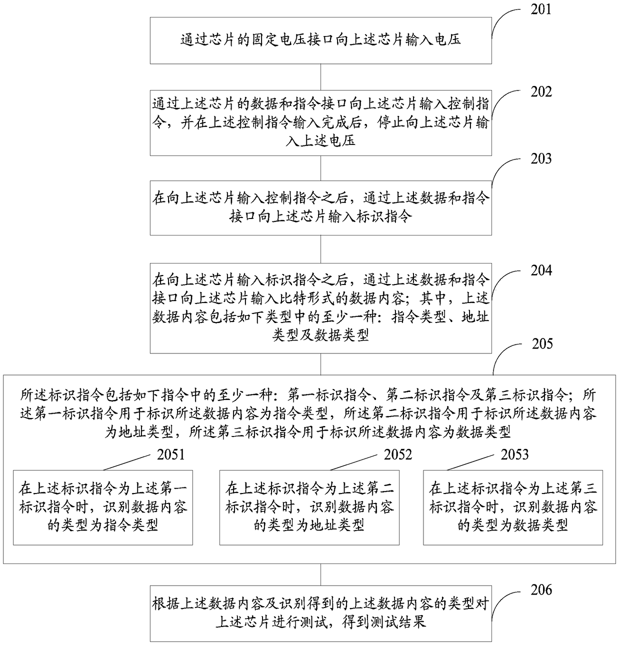
[0070] refer to figure 2 , shows a flow chart of the steps of Embodiment 2 of a test method of the present invention, which may specifically include the following steps:
[0071] Step 201, inputting a voltage to the chip through a fixed voltage interface of the chip;
[0072] Step 202: Input a control command to the chip through the data and command interface of the chip, and stop inputting the voltage to the chip after the input of the control command is completed;
[0073] Step 203, after inputting the control instruction to the above-mentioned chip, input the identification instruction to the above-mentioned chip through the above-mentioned data and instruction interface;
[0074] Step 204, after inputting the identification instruction to the above-mentioned chip, input the data content in bit form to the above-mentioned chip through the above-mentioned data and instruction interface; wherein, the above-mentioned data content includes at least one of the following types:...
Embodiment 3
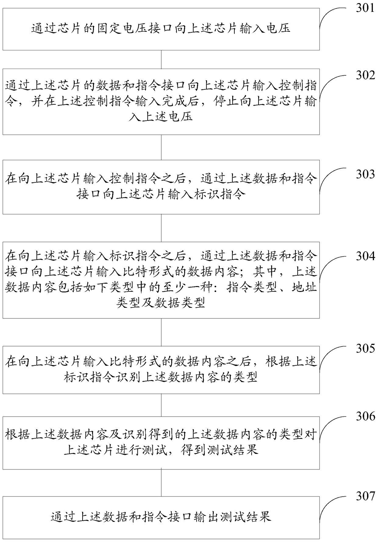
[0081] refer to image 3 , shows a flow chart of the steps of Embodiment 3 of a test method of the present invention, which may specifically include the following steps:
[0082] Step 301, inputting a voltage to the chip through a fixed voltage interface of the chip;
[0083] Step 302: Input a control command to the chip through the data and command interface of the chip, and stop inputting the voltage to the chip after the input of the control command is completed;
[0084] Step 303, after inputting the control instruction to the above-mentioned chip, input the identification instruction to the above-mentioned chip through the above-mentioned data and instruction interface;
[0085] Step 304, after inputting the identification instruction to the above-mentioned chip, input the data content in bit form to the above-mentioned chip through the above-mentioned data and instruction interface; wherein, the above-mentioned data content includes at least one of the following types: ...
PUM
 Abstract
Description
Claims
Application Information
 - R&D
- Intellectual Property
- Life Sciences
- Materials
- Tech Scout
- Unparalleled Data Quality
- Higher Quality Content
- 60% Fewer Hallucinations
Browse by: Latest US Patents, China's latest patents, Technical Efficacy Thesaurus, Application Domain, Technology Topic, Popular Technical Reports.
© 2025 PatSnap. All rights reserved.Legal|Privacy policy|Modern Slavery Act Transparency Statement|Sitemap|About US| Contact US: help@patsnap.com