Supercharge Your Innovation With Domain-Expert AI Agents!

Circuit and method for suppressing negative voltage of bit line under high power supply voltage

A power supply voltage and negative voltage technology, applied in the electronic field, can solve problems such as voltage difference, leakage, gate oxide layer breakdown, etc., and achieve the effect of avoiding damage

Active Publication Date: 2019-06-25
SPREADTRUM COMM (SHANGHAI) CO LTD
View PDF7 Cites 2 Cited by
  • Summary
  • Abstract
  • Description
  • Claims
  • Application Information

AI Technical Summary

Problems solved by technology

[0005] However, the use of bit line negative voltage technology will cause the gate oxide layer of the MOS transistor on the SRAM bit line path to withstand a large voltage difference when the power supply voltage is high, which may cause breakdown or leakage of the gate oxide layer

Method used


Image

  • Circuit and method for suppressing negative voltage of bit line under high power supply voltage
  • Circuit and method for suppressing negative voltage of bit line under high power supply voltage
  • Circuit and method for suppressing negative voltage of bit line under high power supply voltage

Examples


specific Embodiment

[0129] A specific embodiment, taking the step of writing data 0 as an example: refer to Figure 9 ,include:

[0130] Step s11, the first bit line BL is pulled down to the ground voltage VSS;

[0131] Step s12, the first external signal NBSTEB changes from high level to low level, and the first signal NBST0 changes from high level to low level after a delay of the first set time t1 and is transmitted on the first bit line BL Coupling generates a negative voltage; the first write enable signal WT0 delays the second set time t2 and disconnects the connection between the first bit line BL and the ground voltage. When the power supply voltage is a high power supply voltage, it is coupled on the first bit line BL After obtaining the negative voltage, disconnect the first bit line BL from VSS of the ground voltage to obtain the ground voltage VSS on the first bit line BL;

[0132] Step s13 , the word line of one of the N SRAM memory cells is selected, the first bit line BL is connect...


PUM


Abstract

The invention relates to the field of the electronic technology, in particular to a circuit for inhibiting a negative bit line under high supply voltage. The circuit comprises N SRAM (Static Random Access Memory) storage units, a detection unit and a control unit, wherein each SRAM storage unit is connected with a first bit line, a second bit line and a corresponding word line, and carries out a write operation on the corresponding SRAM storage unit when one word line is selected; the detection unit is used for detecting the power voltage of each SRAM storage unit, and generates a regulation signal according to the change of the power voltage; and the control unit is connected with the detection unit, and is regulated by the regulation signal to enable negative voltage obtained by coupling on a first bit line or a second bit line to be grounded when the power voltage exceeds a threshold value. By use of the circuit, through regulation, the negative voltage obtained by coupling on the first bit line or the second bit line is grounded when the power voltage rises, the damage of the gate oxide of a MOS (Metal Oxide Semiconductor) transistor on a bit line passage is avoided, the inhibition of the negative bit line during high voltage is realized, a circuit is simple, and the area of the circuit is saved.

Description

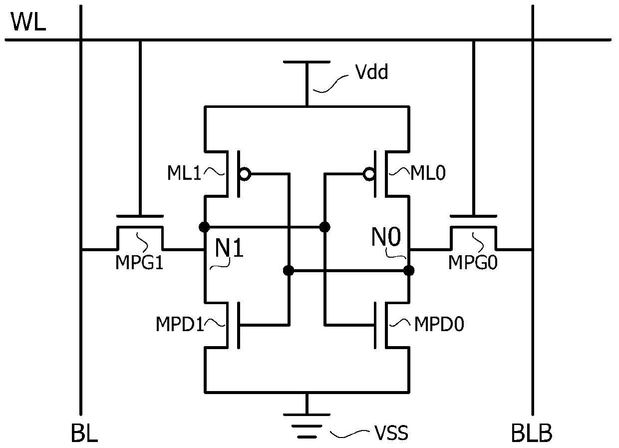
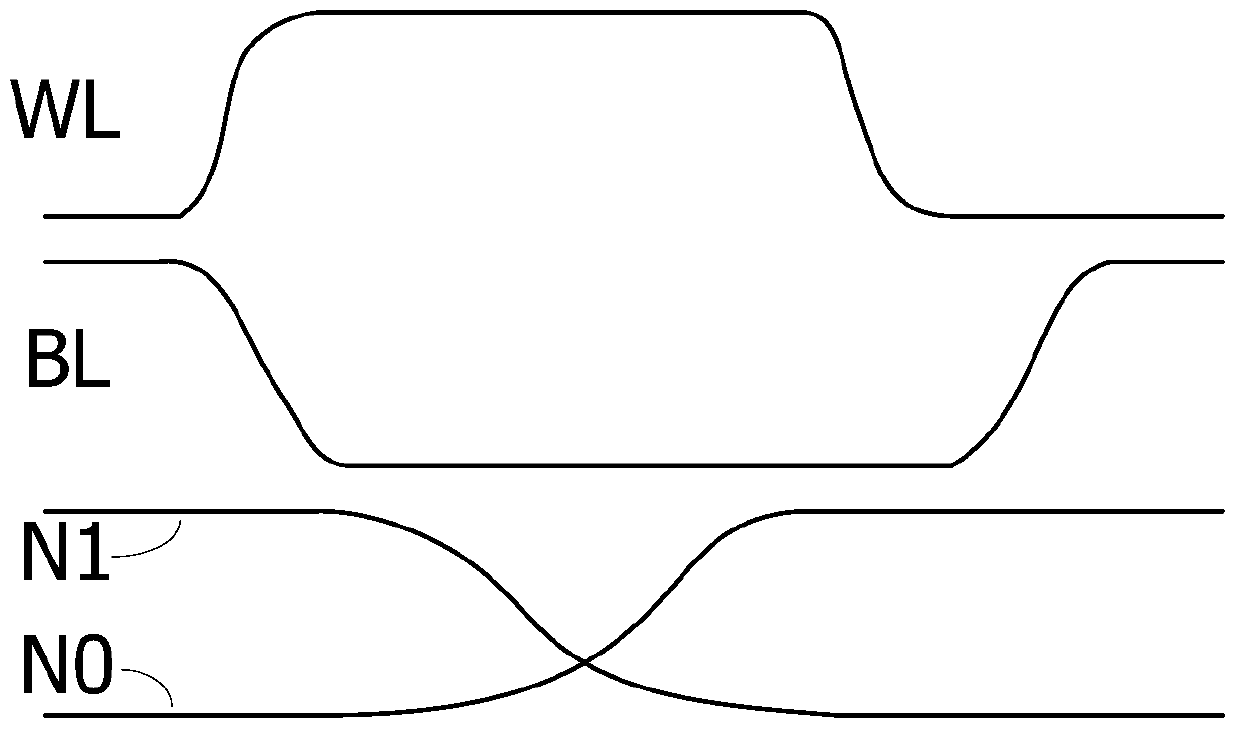
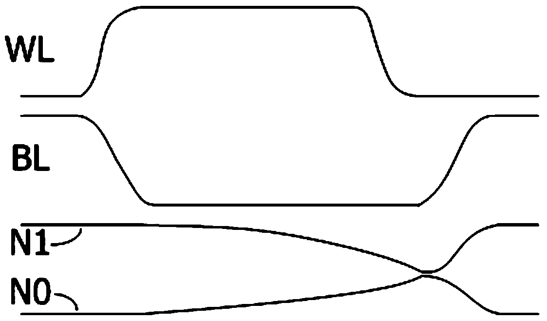
technical field [0001] The invention relates to the field of electronic technology, in particular to a static random access memory. Background technique [0002] The most common structure of SRAM is as figure 1 As shown, the SRAM storage unit composed of six transistors has a circuit principle: when the voltage of node N1 is high and the voltage of node N0 is low, the value stored in the storage unit is called logic 1, otherwise it is logic 0. When it is necessary to rewrite the data stored in the SRAM storage unit, for example, rewrite the stored value 1 to 0, the corresponding operation steps are: first, charge the word line WL (WordLine) to a high voltage (generally equal to the power supply voltage Vdd), and turn the bit The voltage of the line BL (BitLine) is pulled down from the power supply voltage Vdd to the ground voltage VSS, while the voltage of the reverse bit line BLB is maintained at the power supply voltage Vdd; since the driving ability of the PMOS transisto...

Claims


Application Information

Patent Timeline
Patent Type & Authority Patents(China)
IPC IPC(8): G11C11/413
Inventor 王林
Owner SPREADTRUM COMM (SHANGHAI) CO LTD
Features
  • R&D
  • Intellectual Property
  • Life Sciences
  • Materials
  • Tech Scout
  • Unparalleled Data Quality
  • Higher Quality Content
  • 60% Fewer Hallucinations
Learn More