Method for electroplating copper taphole in PCB

A technology of electroplating copper and plugging holes, which is applied in the direction of electrical components, printed circuits, printed circuits, etc., to achieve the effects of reducing the number of grinding boards, reducing delamination explosion, and reducing the degree of expansion and contraction

Inactive Publication Date: 2017-02-22
SHENZHEN SUNTAK MULTILAYER PCB
View PDF3 Cites 6 Cited by
  • Summary
  • Abstract
  • Description
  • Claims
  • Application Information

AI Technical Summary

Problems solved by technology

[0003] The present invention aims at the problem that it is difficult for the existing plug hole technology to make the through-hole sag less than or equal to 3 μm after filling, and provides a method for electroplating copper plug holes in PCBs. The depression at the hole after the plug hole is less than or equal to 3μm

Method used


Image

  • Method for electroplating copper taphole in PCB
  • Method for electroplating copper taphole in PCB

Examples


Embodiment 1

[0022] This embodiment provides a method for manufacturing a PCB. It is necessary to manufacture copper plug holes on the PCB to fill the metallized through holes by means of electroplating copper. And in order to illustrate the technical content of the present invention, the holes on the PCB of this embodiment are designed to be copper plug holes, and there is no need to make other metallized holes and metallized holes filled with other materials.

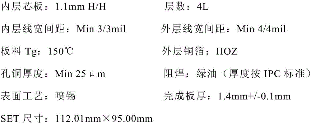
[0023] The specification parameters of the prepared PCB are as follows:

[0024]

[0025] Specific steps are as follows:

[0026] (1) Multi-layer production board

[0027] According to the existing technology, the inner layer core board and the outer layer copper foil are made into a multi-layer production board through the process of material cutting → negative film making of the inner layer circuit → pressing → drilling → copper sinking → full board electroplating, that is, the inner layer core board and the outer layer copp...

Embodiment 2

[0062] This embodiment provides a method for manufacturing a PCB. It is necessary to manufacture copper plug holes on the PCB to fill the metallized through holes by means of electroplating copper. In addition to the copper plug holes, other metallized holes (such as metallized through holes and metallized blind holes) need to be formed on the PCB of this embodiment.

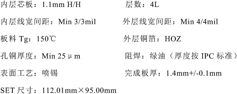
[0063] The specification parameters of the prepared PCB are as follows:

[0064]

[0065] Specific steps are as follows:

[0066] (1) Multi-layer production board

[0067] According to the existing technology, the inner layer core board and the outer layer copper foil are made into a multi-layer production board through the process of material cutting → negative film making of the inner layer circuit → pressing → drilling → copper sinking → full board electroplating, that is, the inner layer core board and the outer layer copper foil are made into a multi-layer production board The core board, the prepreg a...


PUM


Abstract

The invention relates to the technical field of circuit board production, in particular to a method for an electroplating copper taphole in a PCB. The method comprises the steps of forming a first metalized blind hole from a first surface of a multi-layer working panel, forming a second metalized bind hole from a second surface, making the bottom of the first metalized blind hole connect with the bottom of the second metalized blind hole in a butt-joint mode so that an existing porefilling electroplating production line can be used to conduct via-filling-plating on the first metalized blind hole and the second metalized bind hole and finally forming the copper taphole tamped by electroplating copper. The advantages that roasting is not needed by the electroplating copper taphole and a stuffing material coincides with a hole wall metal are used to solve the problem that a porthole sunken depth is larger than 3 micrometers caused by roasting in the prior art; meanwhile, due to the fact that copper is used as the stuffing material and expansion coefficient of the stuffing material coincides with that of a hole wall copper layer can sharply lower risks of stratified plate blasting in a welding process. The number of plate grinding times in a production process can be lowered by using the electroplating copper to tamp metalized through holes, thus expansion-shrinkage degree of the multi-layer working panel can be lowered; meanwhile, the method is beneficial to improvement of the quality of the product.

Description

technical field [0001] The invention relates to the technical field of circuit board production, in particular to a method for electroplating copper plug holes in a PCB. Background technique [0002] PCB (Printed Circuit Board), the Chinese name is printed circuit board, also known as printed circuit board. The production of PCB includes two links of circuit design and manufacturing. The manufacture of PCB is based on the previous circuit design. The manufacturing process is generally as follows: according to the design requirements, the inner core board is cut into the required size in the cutting process→inside Lay film on the core board → use the inner layer film to expose in position → develop and remove the uncured film to form an inner layer pattern → etch the copper layer not covered by the film on the inner core board to form an inner layer circuit → fade the film → put The inner core boards are stacked in a certain order and combined by high temperature pressure to...

Claims


Application Information

Patent Timeline
Patent Type & Authority Applications(China)
IPC IPC(8): H05K3/42
CPCH05K3/421H05K2201/09563H05K2203/107
Inventor 周文涛彭卫红翟青霞宋清
Owner SHENZHEN SUNTAK MULTILAYER PCB
Why Eureka
Try Eureka