Blind hole window manufacturing method capable of improving unfilled hole filling

A manufacturing method and a window-opening technology, which are applied in multilayer circuit manufacturing, printed circuit manufacturing, electrical components, etc., can solve the problems of blind holes being offset and tangent, deep depressions, and inability to fill, etc. The effect of reducing scrap and saving costs

Active Publication Date: 2017-02-22
SHENZHEN SUNTAK MULTILAYER PCB
View PDF4 Cites 6 Cited by
  • Summary
  • Abstract
  • Description
  • Claims
  • Application Information

AI Technical Summary

Problems solved by technology

[0005] 1. When filling the hole, the two ends of the window of the blind hole are deeply depressed and cannot be filled;
[0006] 2. When mechanical drilling and laser drilling exist at the same time, because two sets of expansion and contraction coefficients are involved, the blind hole will have an offset and tangent effect after the graphics are aligned with the drilling CCD;
[0007] 3. During etching, because the recessed blind hole is tangent to the edge of the pad, the hole cannot be sealed, resulting in the quality problem of etching the pad away
[0009] However, the above-mentioned patent achieves the purpose of precise window opening in blind holes by avoiding the repeated use of the outer pipe position holes and mechanical drilling errors, which is relatively difficult

Method used


Image

  • Blind hole window manufacturing method capable of improving unfilled hole filling
  • Blind hole window manufacturing method capable of improving unfilled hole filling
  • Blind hole window manufacturing method capable of improving unfilled hole filling

Examples


Embodiment Construction

[0035] In order to fully understand the technical content of the present invention, the technical solutions of the present invention will be further introduced and illustrated below in conjunction with specific examples, but not limited thereto.

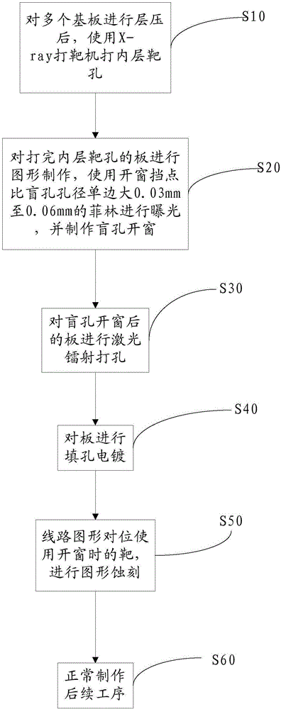
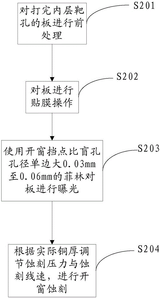
[0036] like Figure 1~2 As shown in the specific embodiment, this embodiment provides a blind hole opening method for improving incomplete hole filling, which can be used in the hole filling process of printed circuit boards to reduce window opening and reduce hole filling by electroplating. The difficulty of leveling, thus greatly reducing the scrapping of pad etching caused by poor sealing of blind holes when making outer graphics, saving costs and reducing scrapping. Specifically, it can be used in the production process of various multi-layer boards.

[0037] A blind hole window manufacturing method for improving insufficiency of hole filling, comprising the following steps:

[0038] S10. After laminating multiple substrates, u...


PUM


Abstract

The invention relates to a blind hole window manufacturing method capable of improving unfilled hole filling. The blind hole window manufacturing method comprises the following steps: laminating a plurality of base plates, and then punching an inner-layer target hole by adopting an X-ray target shooting machine; manufacturing a graph on the plate subjected to inner-layer target hole punching, carrying out exposure by utilizing a film with a window stopping point which is 0.03mm to 0.06mm larger than a single edge of the hole diameter of a blind hole, and manufacturing a blind hole window; carrying out laser punching on the plates with the blind hole windows; carrying out hole filling electroplating on the plates; carrying out graph etching by utilizing a target for forming the window in a line graph alignment process; and normally carrying out a subsequent manufacturing procedure. According to the blind hole window manufacturing method provided by the invention, the problem that the hole filling is not full is solved through reducing the sizes of the blind hole windows; when through holes and the blind hole exist at the same time, graphs are aligned by utilizing a blind hole alignment hole and the quality of the blind hole is guaranteed preferably, so that the quality problem that the pad in a tangent position of the blind hole and pad is etched can be avoided; and pad etching rejection caused by the fact that hole sealing of a blind hole sticking film is not good when an outer-layer graph is manufactured is greatly reduced, the cost is saved, and the rejection rate is reduced.

Description

technical field [0001] The invention relates to a printed circuit board, and more specifically refers to a method for making blind holes and opening windows to improve filling holes. Background technique [0002] Printed circuit board (PCB) appears in almost every electronic device. If there are electronic parts in a certain device, they are also mounted on PCBs of various sizes. In addition to fixing various small parts, the main function of the PCB is to provide electrical connections between the various parts above. As electronic devices become more and more complex, more and more parts are required, and the lines and parts on the PCB are becoming more and more dense. [0003] In the production process of printed circuit boards, when the customer requires the use of copper foil of more than 0.5 ounces for pressing and plating, and laser blind hole filling and electroplating, generally the blind hole production method of direct laser copper plating cannot be used, but it...

Claims


Application Information

Patent Timeline
Patent Type & Authority Applications(China)
IPC IPC(8): H05K3/46
CPCH05K3/4614H05K2203/052H05K2203/107
Inventor 陈则鸣董猛荣孝强
Owner SHENZHEN SUNTAK MULTILAYER PCB
Why Eureka
Try Eureka