Shock absorption apparatus and circuit board assembly

A shock-absorbing device and circuit board technology, which is applied in the electronic field, can solve problems such as high thermal expansion rate, rubber aging, and loss of vibration protection, and achieve the effect of reducing vibration amplitude and vibration impact

Inactive Publication Date: 2017-02-22
FUDAN UNIV
View PDF7 Cites 7 Cited by
  • Summary
  • Abstract
  • Description
  • Claims
  • Application Information

AI Technical Summary

Problems solved by technology

[0005] However, in the process of realizing the present invention, the inventors of the present application found that the underfill solution has the following problems: (1) the underfill is usually a poor conductor, which is not good for the heat dissipation of active devices; (2) the underfill The thermal expansion rate of the device is larger than that of the device, which may cause additional thermal stress at high temperature; (3) In some harsh environments, such as applications with high temperature and long time, the problem of rubber aging is prone to occur, and the vibration protection effect is lost
The scheme of connecting with a spring piece makes the distance between the device and the PCB relatively large, which increases the occupied area of ​​the device, which is not conducive to the current trend of high integration
The chassis and shock-absorbing ring scheme with springs increase the shock-absorbing structure, which not only increases the cost, but also is not compatible with most PCB surface-mounted device structures
Springs and non-metal material buffer devices can alleviate the vibration transmitted from the vibration source to the fixed object through a fixed position, but the non-metal film is added for buffering, which is not stable enough and the structure is relatively complicated

Method used


Image

  • Shock absorption apparatus and circuit board assembly
  • Shock absorption apparatus and circuit board assembly
  • Shock absorption apparatus and circuit board assembly

Examples


Embodiment Construction

[0025] In order to make the object, technical solution and advantages of the present invention clearer, various embodiments of the present invention will be described in detail below in conjunction with the accompanying drawings. However, those of ordinary skill in the art can understand that, in each implementation manner of the present invention, many technical details are provided for readers to better understand the present application. However, even without these technical details and various changes and modifications based on the following implementation modes, the technical solution claimed in this application can also be realized.

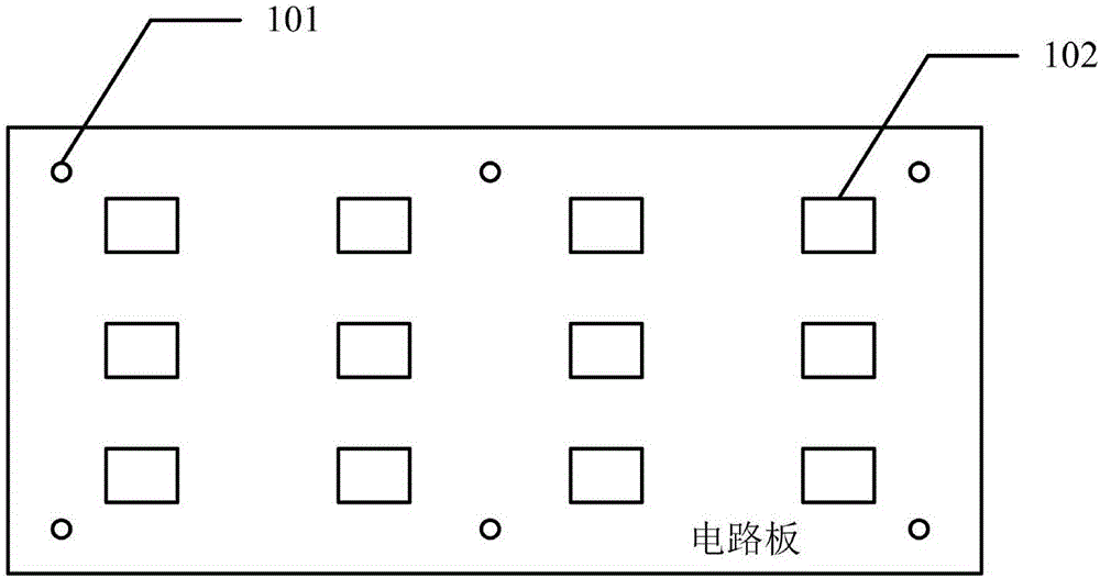
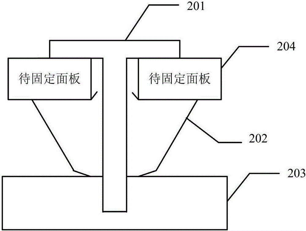
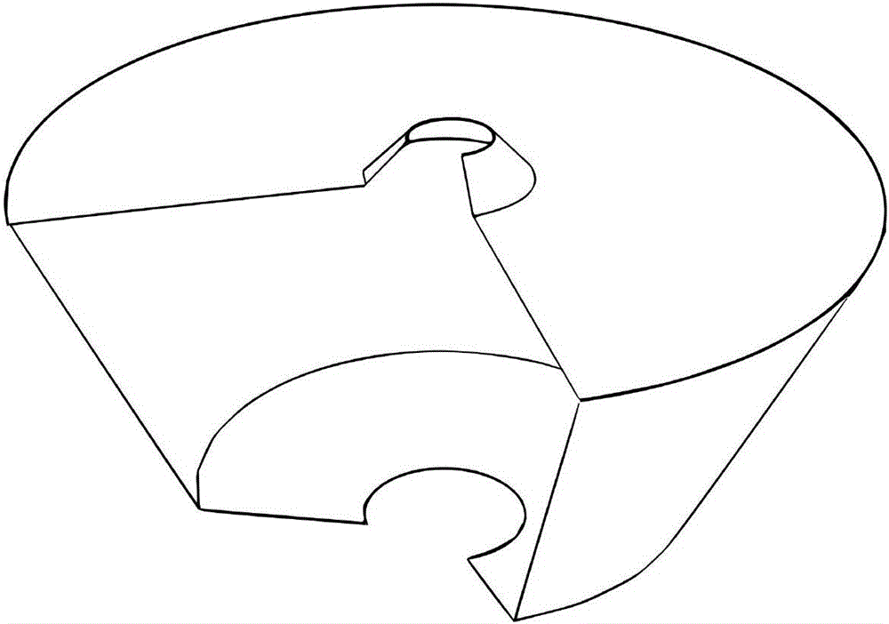
[0026] A first embodiment of the present invention relates to a shock absorber. The specific structure diagram is as figure 2 shown. It includes: a fixing piece 201 , a shock absorbing device 202 , a fixing plane 203 and a panel 204 to be fixed.

[0027] The fixing member 201 is used for passing through the fixing hole of the panel to b...


PUM


Abstract

The invention relates to the electronic technical field, and discloses a shock absorption apparatus and a circuit board assembly. According to the embodiments of the invention, the first surface of the shock absorption apparatus with a hollow interior is in contact with a to-be-fixed panel equipped with at least one fixing hole while the second surface of the shock absorption apparatus is in contact with a fixed plane, so that the shock absorption apparatus is positioned between the to-be-fixed panel and the fixed plane; and the to-be-fixed panel passes through the fixing hole and the shock absorption apparatus through a fixing part to be fixed on the fixed plane, so that the shock absorption apparatus is positioned between the fixing hole of the to-be-fixed panel and the fixed plane. According to the embodiments of the invention, by additionally arranging the shock absorption apparatus between the fixing hole of the to-be-fixed panel and the fixed plane, vibration buffering between the to-be-fixed panel and the fixed plane is formed, so that the vertical vibration amplitude transferred to the to-be-fixed panel through the fixing part is lowered, and the vibration impact on the overall to-be-fixed panel is weakened.

Description

technical field [0001] The invention relates to the field of electronic technology, in particular to a shock absorbing device and a circuit board assembly. Background technique [0002] In the process of assembling microelectronic packaging devices into printed circuit boards (Print Circuit Board), the connection between devices and PCB is usually in the form of solder ball array BGA (Ball GridArray) or pins, and electrical and mechanical connections are realized by soldering. A variety of devices are often installed on the PCB, and the size of the devices is relatively small, on the order of centimeters to millimeters. It is difficult and uneconomical to design shock absorption for a single device. [0003] Usually, the PCB passes through the fixing hole through the fixing part and is fixed in a plane position. The vibration is mainly transmitted to the PCB through the fixing part, and then affects the reliability of the soldering point of the device, such as figure 1 As s...

Claims


Application Information

Patent Timeline
Patent Type & Authority Applications(China)
IPC IPC(8): H05K7/12
Inventor 王珺赵立有杨辰
Owner FUDAN UNIV
Why Eureka
Try Eureka