Supercharge Your Innovation With Domain-Expert AI Agents!

Method for producing bonded body

A manufacturing method and technology of bonding body, which are applied in the direction of semiconductor/solid-state device manufacturing, semiconductor device, electric solid-state device, etc.

Active Publication Date: 2017-02-22
SHINDENGEN ELECTRIC MFG CO LTD
View PDF5 Cites 0 Cited by
  • Summary
  • Abstract
  • Description
  • Claims
  • Application Information

AI Technical Summary

Problems solved by technology

[0006] However, in the above-mentioned method, heat is conducted from the first heating plate 920 to the metal particle paste 16 due to heat conduction before the assembly 10 is pressurized, thereby causing the metal particle paste 16 to partially initiate a sintering reaction (curing reaction), which As a result, there is a problem that the substrate 12 on which the conductor circuit pattern is formed and the semiconductor element 14 cannot be bonded with high bonding force.
[0007] Furthermore, such a problem will not only occur when manufacturing a semiconductor device having a structure in which a substrate having a conductive circuit pattern formed using a metal particle paste is bonded to a semiconductor element, but will occur when a substrate having a conductive circuit pattern formed using a metal particle paste is used. Graphical substrates, other substrates] and [other electronic components of semiconductor elements] are bonded to all junctions of the structure

Method used


Image

  • Method for producing bonded body
  • Method for producing bonded body
  • Method for producing bonded body

Examples


Embodiment approach 1

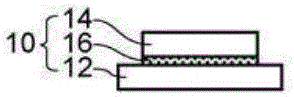
[0040] As shown in FIG. 1 , the method of manufacturing a bonded body according to Embodiment 1 is a method of manufacturing a structure in which a substrate 12 (a substrate on which a conductive circuit pattern is formed) and an electronic component 14 (semiconductor element) are bonded via a metal particle paste 16 . A method of manufacturing a bonded body 11 (semiconductor device) (a method of manufacturing a semiconductor device).

[0041] Next, the substrate 12, the electronic component 14, and the metal particle paste 16 will be described in detail.

[0042] The "substrate" in the present invention refers to a component on which electronic components are mounted.

[0043]Electronic components 14 are mounted on the substrate 12 . The substrate 12 in Embodiment 1 is, for example, a circuit substrate in which a conductive circuit pattern is formed on a body made of a non-conductive material. As the constituent material of the substrate 12, a material (for example, a heat-...

Embodiment approach 2

[0065]The method of manufacturing the joined body in Embodiment 2 basically includes the same steps as the method of manufacturing the joined body in Embodiment 1, but it differs from the method of manufacturing the joined body in Embodiment 1 in that it does not utilize two The sheet heating plate directly pressurizes and heats the assembly to join the substrate and the electronic component, but indirectly presses and heats the assembly using a pressing unit to join the substrate and the electronic component. That is, the manufacturing method of the bonded body in Embodiment 2, as shown in FIG. 5 , between the assembly forming step and the assembly arranging step, further includes: a pressurizing unit forming step, so as to utilize the two functions of conducting pressure and heat. The sheet conduction members (first conduction member 210, second conduction member 220) sandwich the assembly to form a press unit 200 (see FIG. 5(a)), which is characterized in that: In the proce...

Embodiment approach 3

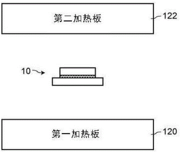
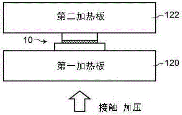
[0098] The method of manufacturing a joined body according to Embodiment 3 basically includes the same steps as the method of manufacturing a joined body in Embodiment 1, but it differs from the method of manufacturing a joined body in Embodiment 1 in that the first heating plate The temperature and the content of the assembly configuration process. That is, in the method for manufacturing a bonded body according to the third embodiment, the temperature of the first heating plate 120 among the two heating plates is set in the range of 50° C. to 150° C. (for example, 100° C.), and the two heating plates are The temperature of the second heating plate 122 among the heating plates is set in the range of 250° C. to 350° C. (for example, 300° C.), and, in the assembly disposing process, the assembly 10 is arranged on the same side as the first heating plate 120 . contact position (refer to Figure 11).

[0099] In this way, the method of manufacturing a bonded body according to the t...


PUM


Abstract

Disclosed is a bonded body production method for producing a bonded body having a structure in which a substrate and an electronic component are bonded by means of a metal particle paste, the method comprising: an assembly forming step for forming an assembly in which an electronic component is placed on a substrate with a metal particle paste therebetween; an assembly arranging step for arranging the assembly between two heating plates; and a bonding step for bonding the substrate and the electronic component together by heating the assembly while pressurizing the same by moving at least one of the two heating plates toward the other. In this bonded body production method, the bonding step is performed under a condition where the temperature of the assembly at the time of starting the pressurization of the assembly with the two heating plates is within the range of from 0 DEG C to 150 DEG C. According to this bonded body production method, because the bonding step is performed under a condition where the temperature of the assembly at the time of starting pressurization is within the range of from 0 DEG C to 150 DEG C, the metal particle paste is less likely to undergo a sintering reaction before pressurizing the assembly in the bonding step, and as a result, the substrate and the electronic component can be bonded together with higher bonding force than before.

Description

technical field [0001] The present invention relates to a method for producing a bonded body. Background technique [0002] Conventionally, a semiconductor device has been generally known, which has a structure in which a substrate on which a conductor circuit pattern is formed is bonded to a semiconductor element using metal particle paste (for example, refer to Patent Document 1). The metal particle slurry contains nano-size or submicron-size metal particles in a solvent, and utilizes the low-temperature sintering phenomenon of metal particles and low-temperature sintering after high surface activity. Conductive paste. [0003] The above-mentioned semiconductor device, as shown in FIG. 18, is carried out by carrying out: the assembly 10 (refer to FIG. 18 (a)) in which the semiconductor element 14 is placed on the substrate 12 on which the conductor circuit pattern is formed with the metal particle slurry 16, is mounted. After placing the upper side of the first heating p...

Claims


Application Information

Patent Timeline
IPC IPC(8): H01L21/52
CPCH01L24/75H01L2224/75314H01L2224/75754H01L24/29H01L24/32H01L2224/29339H01L2224/29344H01L2224/29347H01L2224/32227H01L2224/32245H01L2224/7525H01L2224/75251H01L2224/75252H01L2224/753H01L2224/7565H01L2224/83204H01L2224/8384H01L2224/75704H01L2224/29294H01L24/83H01L2924/00014H01L2924/00012H01L21/52H01L2224/83203H01L2224/83986
Inventor 松林良森永雄司
Owner SHINDENGEN ELECTRIC MFG CO LTD
Features
  • R&D
  • Intellectual Property
  • Life Sciences
  • Materials
  • Tech Scout
  • Unparalleled Data Quality
  • Higher Quality Content
  • 60% Fewer Hallucinations
Learn More