Light modulator, optical module, and image display apparatus

一种光调制器、光调制的技术,应用在光学、光学元件、非线性光学等方向,能够解决光损失、颜色偏差、光导波路光学耦合串扰等问题

Inactive Publication Date: 2017-03-01
SEIKO EPSON CORP
View PDF1 Cites 2 Cited by
  • Summary
  • Abstract
  • Description
  • Claims
  • Application Information

AI Technical Summary

Problems solved by technology

[0014] On the other hand, if the distance between the parallel optical waveguides is too narrow, the optical coupling between the optical waveguides will cause crosstalk, resulting in light loss and color shift.

Method used


Image

  • Light modulator, optical module, and image display apparatus
  • Light modulator, optical module, and image display apparatus
  • Light modulator, optical module, and image display apparatus

Examples


no. 1 approach 》

[0060] First, a first embodiment of the image display device will be described.

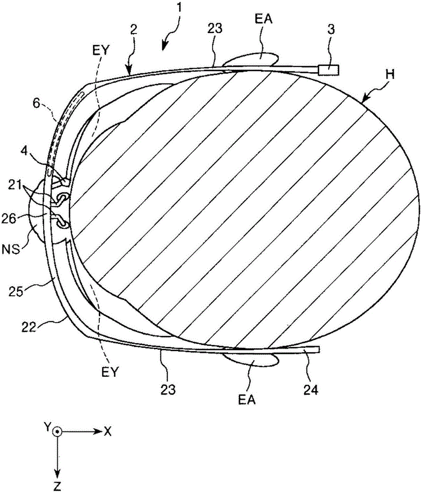
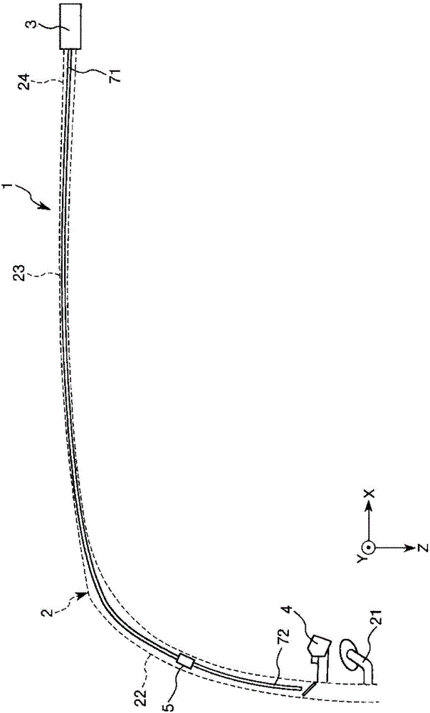
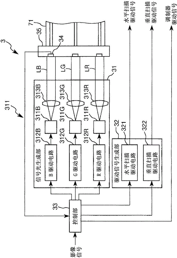
[0061] figure 1 is a diagram showing a schematic configuration of the first embodiment (head-mounted display) of the image display device, figure 2 Yes figure 1 A partial enlarged view of the image display device shown in . and, image 3 Yes figure 1 A schematic configuration diagram of the signal generation unit of the image display device shown in , Figure 4 is showing figure 1 A diagram showing a schematic configuration of the light scanning section included in the scanning light emitting section, Figure 5 is used to illustrate figure 1 A diagram of the action of the image display device shown in . and, Image 6 It is a diagram showing the scanning trajectory of the signal light on the imaging plane according to the first embodiment. and, Figure 7 is showing Figure 4 A perspective view of the schematic configuration of the modulator shown in, Figure 8 Yes Figure 7 The top ...

no. 2 approach 》

[0223] Next, a second embodiment of the image display device will be described.

[0224] Figure 9 It is a plan view showing a schematic configuration of a modulator included in the image display device according to the second embodiment.

[0225] Hereinafter, although the second embodiment will be described, in the following description, the differences from the above-mentioned first embodiment will be mainly described, and the description of the same items will be omitted. In addition, the same symbols are assigned to the same items in the drawings as those in the above-mentioned embodiment.

[0226] like Figure 9 As shown, in the modulator 30 according to the second embodiment, the distribution branch portion 3027B (first branch portion) is provided between the incident portion 3021B of the optical waveguide 302B and the modulation branch portion 3022B. As a result, the optical waveguide 302B branches into two in the vicinity of the incident portion 3021B. As a result,...

no. 3 approach 》

[0257] Next, a third embodiment of the image display device will be described.

[0258] Figure 11 It is a plan view showing a schematic configuration of a modulator included in an image display device according to a third embodiment.

[0259] Hereinafter, although the third embodiment will be described, in the following description, the differences from the above-mentioned first and second embodiments will be mainly described, and the description of the same items will be omitted. In addition, the same symbols are assigned to the same items in the drawings as those in the above-mentioned embodiment.

[0260] like Figure 11 As shown, in the modulator 30 according to the third embodiment, between the incident part 3021B of the optical waveguide 302B and the modulation branch part 3022B, the primary distribution branch part 3028B, the two Secondary dispensing fork 3029B. Specifically, the main line 3020B (first main line) of the optical waveguide 302B is bifurcated into two...


PUM


Abstract

The invention discloses a light modulartor with small emited light beam distance and less light loss, an optical module having the light modulator and an image display apparatus.A light modulator (3) includes a substrate (301) providing an electro-optical effect and provided with first to third optical waveguides (302B,302G,302R), a first modulation section (300B) that modulates a blue light (LB) flux passing through the first optical waveguide (302B), a second modulation section (300G) that modulates a green light flux (LG) passing through the second optical waveguide (302G), and a third modulation section (300R) that modulates a red light flux (LR) passing through the third optical waveguide (302R), and L1<L2<L3 and S1>S2>S3 are satisfied, where L1 represents the length of the first modulation section (300B), S1 represents the distance between a first reference line (DL1) and a first exit section (3026B), L2 represents the length of the second modulation section (300G), S2 represents the distance between a second reference line (DL2)and a second exit section (3026R), L3 represents the length of the third modulation section (300R), and S3 represents the distance between a third reference line (DL3)and a third exit section (3026R).

Description

technical field [0001] The invention relates to a light modulator, an optical module and an image display device. Background technique [0002] Head-mounted displays (HMDs) and head-up displays (HUDs) are known as display devices that directly irradiate laser light to the retina of pupils to allow users to recognize images. [0003] Such a display generally includes a light emitting device that emits light, and a scanning unit that changes an optical path so that the emitted light scans the user's retina. And, with such a display, the user can simultaneously recognize, for example, both the scenery outside and the image drawn by the scanning unit. [0004] For example, Patent Document 1 discloses a beam scanning display including a light source that emits laser beams of three primary colors, and a deflection unit that scans the laser beams and projects them on a screen. In addition, it is disclosed that a laser beam is deflected in a horizontal direction and a vertical dir...

Claims


Application Information

Patent Timeline
Patent Type & Authority Applications(China)
IPC IPC(8): G02F1/01G02B26/10G02B27/01
CPCG02B26/105G02B27/0172G02F1/011G02B6/00G02B2027/0112G02F1/225G02B27/0101G02B26/101G02B2027/0178G02F1/212
Inventor 冈本纯一
Owner SEIKO EPSON CORP
Why Eureka
Try Eureka