High-frequency, high-output device unit
An equipment device and high-output technology, applied in semiconductor/solid-state device parts, semiconductor devices, electrical components, etc., can solve problems such as solder fracture, achieve the effect of inhibiting development and improving durability
- Summary
- Abstract
- Description
- Claims
- Application Information
AI Technical Summary
Problems solved by technology
Method used
Image

Examples
Embodiment approach 1
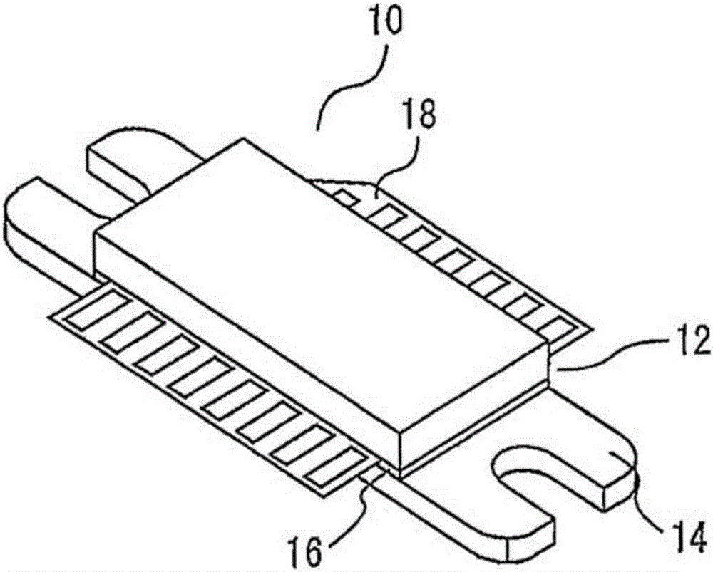
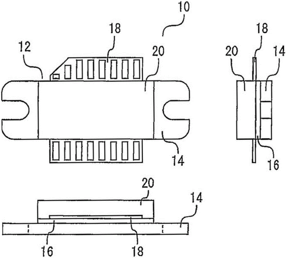
[0028] figure 1 It is a perspective view showing the high-frequency high-output equipment device 10 according to Embodiment 1 of the present invention. figure 2 yes figure 1 Three views of the high-frequency high-output device 10 shown. It is assumed that the high-frequency high-output equipment device 10 of this embodiment has a frequency band of 800 MHz to 3.5 GHz and an output power of 100 W to 300 W, and is used in a mobile phone base station.
[0029] Such as figure 2 As shown, the semiconductor package 12 used in the high-frequency high-output device 10 of the present invention has a base plate 14 . A ceramic frame 16 is mounted on the base plate 14 . Leads 18 for connecting to a circuit board to be mounted are mounted on the ceramic frame 16 . The lead wires 18, the base plate 14, and the ceramic frame 16 were fixed with Ag solder. Furthermore, the ceramic cover 20 is fixed to the upper surface of the ceramic frame 16 with an epoxy resin adhesive.
[0030] Lead...
Embodiment approach 2
[0039] Figure 7 It is a plan view of the high-frequency high-output equipment device 10 according to Embodiment 2 of the present invention, and a cross-sectional view obtained by cutting the device along line VII-VII. This embodiment is the same as Embodiment 1 except that the opening 40 is replaced with the groove 42 . In this embodiment, the concave portion 60 is formed in the planar portion 32 by providing the plurality of grooves 42 in the planar portion 32 . Figure 7 The shown top view is a top view showing the high-frequency high-output equipment device 10 . Therefore, although the groove 42 does not originally appear in the top view, the position of the groove 42 is shown here in the top view with hatching for convenience. The depth of the groove 42 is about half the thickness of the lead 18 . In addition, there are no limitations on the width, depth, cross-sectional shape, and number of grooves.
[0040]According to the present embodiment, similarly to Embodiment...
Embodiment approach 3
[0042] Figure 8 It is a plan view of the high-frequency high-output equipment device 10 according to Embodiment 3 of the present invention. This embodiment is the same as Embodiment 1 except that the opening 44 is vertically longer in the longitudinal direction of the lead wire 18 . In the present embodiment, the concave portion 60 is formed in the planar portion 32 by providing a plurality of openings 44 in the lead wire 18 .
[0043] As in Embodiment 1, contact between the flat portion 32 and the solder 34 is interrupted by the opening 44 , and the stress applied to the portion of the solder 34 that is in contact with the flat portion 32 is reduced. Therefore, the occurrence of cracks can be suppressed.
[0044] In addition, according to the present embodiment, similar to the first embodiment, after a crack has occurred, the linear growth of the crack can be suppressed by the opening 44 . Therefore, the durability related to the breakage of the solder 34 can be improved,...
PUM
 Abstract
Description
Claims
Application Information
 - R&D Engineer
- R&D Manager
- IP Professional
- Industry Leading Data Capabilities
- Powerful AI technology
- Patent DNA Extraction
Browse by: Latest US Patents, China's latest patents, Technical Efficacy Thesaurus, Application Domain, Technology Topic.
© 2024 PatSnap. All rights reserved.Legal|Privacy policy|Modern Slavery Act Transparency Statement|Sitemap