Dual-image-sensor packaging module and formation method therefor

An image sensor and sensor technology, which is used in electric solid-state devices, semiconductor devices, radiation control devices, etc., can solve the problems of low integration of dual cameras and accurate images.

Pending Publication Date: 2017-03-15
CHINA WAFER LEVEL CSP
View PDF4 Cites 6 Cited by
  • Summary
  • Abstract
  • Description
  • Claims
  • Application Information

AI Technical Summary

Problems solved by technology

[0005] However, as people have higher and higher requirements for the clarity of images obtained by cameras, the existing method of obtaining images through a single camera can no longer meet the requirements. For this reason, ...

Method used


Image

  • Dual-image-sensor packaging module and formation method therefor
  • Dual-image-sensor packaging module and formation method therefor
  • Dual-image-sensor packaging module and formation method therefor

Examples


Embodiment Construction

[0066] As mentioned in the background, the existing dual cameras have a low integration level, and the accuracy of acquiring images is limited by the images.

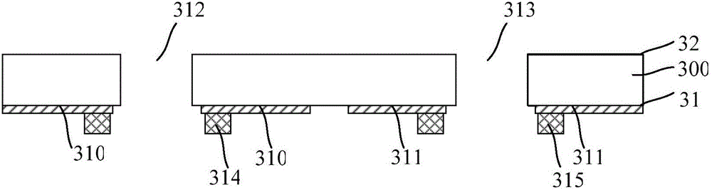
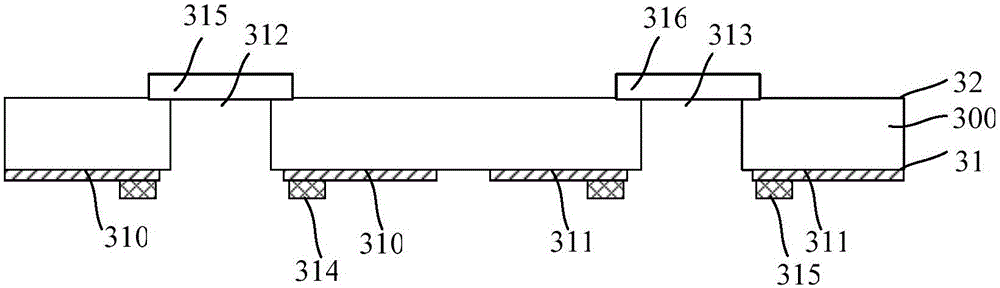
[0067] Research has found that the existing dual cameras are usually implemented by connecting two image sensor modules to the PCB boards of corresponding devices (such as mobile phones), which makes the dual cameras occupy a larger volume and makes the integration of the dual cameras lower. , and when connecting two independent image sensor modules to the PCB board of the corresponding device (such as a mobile phone), the connection process used is usually a welding process, which easily makes the heights of the two image sensor modules inconsistent, thus making the two The heights of the corresponding two image sensors in the image sensor module may be inconsistent, which affects the accuracy of the two image sensors when acquiring images.

[0068] To this end, an embodiment of the present invention provides a dual im...


PUM


Abstract

The invention discloses a dual-image-sensor packaging module and a formation method therefor. The formation method comprises the steps of providing a substrate, wherein the substrate comprises a first surface and a second surface opposite to the first surface, and the substrate has an interconnecting line; providing a first image sensor and a second image sensor, wherein an image sensing region and a bonding pad which surrounds the image sensing region are arranged on the front surface of each of the first image sensor and the second image sensor separately; setting the first image sensor and the second image sensor on the same surface of the substrate, wherein the bonding pad of the first image sensor is electrically connected with the interconnecting line while the bonding pad of the second image sensor is electrically connected with the interconnecting line; and forming welding lug bosses on the first surface and the second surface of the substrate, wherein the welding lug bosses are electrically connected with the interconnecting line; the welding lug bosses are used for being electrically connected with an external circuit; and the convex direction of the welding lug bosses is opposite to the front surface direction of the first image sensor and the second image sensor. By adoption of the scheme, the integration degree of the module is improved while the image acquisition precision is improved.

Description

technical field [0001] The invention relates to semiconductor packaging technology, in particular to a double image sensor packaging structure and a packaging method thereof. Background technique [0002] Image sensors receive light signals from objects and convert them into electrical signals that can be transmitted for further processing, such as digitization, and then stored in a storage device such as memory, optical or magnetic disks, or for display on a display display etc. Image sensors are commonly used in devices such as cell phones, digital cameras, camcorders, scanners, fax machines, and the like. Image sensors generally include charge-coupled device (CCD) image sensors and CMOS image sensors (CIS, CMOS Image Sensor). Compared with CCD image sensors, CMOS image sensors have the advantages of high integration, low power consumption, and low production cost. [0003] An existing image sensor module includes: a substrate, the substrate includes a front surface and...

Claims


Application Information

Patent Timeline
IPC IPC(8): H01L27/146
CPCH01L27/14629H01L27/14634H01L27/14636H01L27/14683
Inventor 王之奇沈志杰罗晓峰
Owner CHINA WAFER LEVEL CSP
Why Eureka
Try Eureka