COB mounting-based optical module circuit board and marking point design

A technology for marking points and circuit boards, applied in the field of optical communication, can solve the problems of high cost of coaxial sockets and caps, inability to guarantee placement accuracy and speed, and cost advantages, etc., to ensure integrity and reliability. Stability, improve accuracy and efficiency, avoid the effect of crosstalk

Inactive Publication Date: 2017-03-15
WUHAN TELECOMM DEVICES
View PDF5 Cites 2 Cited by
  • Summary
  • Abstract
  • Description
  • Claims
  • Application Information

AI Technical Summary

Problems solved by technology

[0003] In the current multi-mode optical module based on the coaxial device solution, in the cost structure, the cost of the coaxial tube base and tube cap accounts for a relatively high proportion, and the room for price reduction is limited
In addition, materials such as coaxial sockets and caps are required, which have no advantages in terms of materials and cost; in terms of technology, the assembly of optical devices and optical modules is required in the process, and the accuracy and speed of placement cannot be guaranteed.

Method used


Image

  • COB mounting-based optical module circuit board and marking point design
  • COB mounting-based optical module circuit board and marking point design

Examples


Embodiment 1

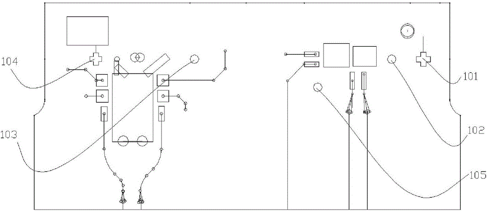
[0038] A design of optical module circuit board and marking points based on COB (CHIP ON BOARD) placement, including: finished circuit board and marking points;

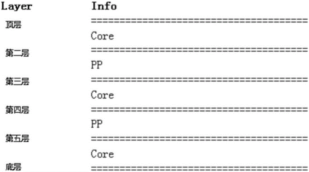
[0039] Pads can be placed on the finished circuit board, and the finished circuit board has six layers of boards, such as figure 2 As shown, from top to bottom are the top layer, the second layer, the third layer, the fourth layer, the fifth layer and the bottom layer;

[0040] The thickness of the finished circuit board is 0.9 mm to 1.1 mm, and the typical thickness of the circuit board is 1.0 mm; from top to bottom are the top layer, the second layer, the third layer, the fourth layer, the fifth layer and the bottom layer; the bottom layer The circuit board is convenient to design the power layer and the ground layer, avoiding crosstalk caused by the routing of the wiring layer, and ensuring the integrity and stability of the signal.

[0041] The finished circuit board has a certain degree of warpage, and the deg...


PUM


Abstract

The invention provides COB mounting-based optical module circuit board and marking point design. A finished circuit board and marking points are included; bonding pads can be placed on the finished circuit board; the finished circuit board is provided with a six-layer board, including a top layer, a second layer, a third layer, a fourth layer, a fifth layer and a bottom layer from top to bottom in sequence; the marking points can recognize the position of the finished circuit board; the number of the marking points is five; in the optical module design of the COB scheme, a bare chip is directly mounted on the circuit board, and the circuit board replaces a conventional transitional block, so that mounting equipment is required for chip mounting, and routing equipment is required for routing a gold wire; and therefore, compared with a conventional circuit board, the circuit board used for the COB scheme needs to satisfy recognition requirement of the mounting equipment on the marking points, and the binding pulling force requirement of the wiring equipment on bonding pad routing.

Description

technical field [0001] The invention belongs to the field of optical communication, and in particular relates to a design of an optical module circuit board and marking points based on COB placement. Background technique [0002] Small form-factor hot-swappable modules are miniaturized pluggable optical modules used in data centers, cloud computing, and fiber channel systems. The design purpose of this module is to provide higher access density through smaller size and lower cost, and ultimately increase user access capacity. [0003] In the current multi-mode optical module based on the coaxial device solution, in the cost structure, the cost of the coaxial socket and cap accounts for a relatively high proportion, and the room for price reduction is limited. In addition, materials such as coaxial sockets and caps are required, which has no advantages in terms of materials and cost; in terms of technology, the assembly of optical devices and optical modules is required in t...

Claims


Application Information

Patent Timeline
Patent Type & Authority Applications(China)
IPC IPC(8): H05K1/02H05K1/18
CPCH05K1/0266H05K1/0216H05K1/181
Inventor 秦艳杨昌霖倪鹏远张南陈志娥
Owner WUHAN TELECOMM DEVICES
Why Eureka
Try Eureka