Exciplex-based organic electroluminescent device and preparation method thereof

A technology of electroluminescent devices and exciplexes, which is applied in the direction of electric solid-state devices, semiconductor/solid-state device manufacturing, electrical components, etc., can solve the problem of increasing device operating voltage, unfavorable carrier injection, low carrier Mobility and other issues, to achieve the effect of reducing the operating voltage, reducing the concentration quenching effect, and improving the transmission capacity

Active Publication Date: 2018-09-25
SUZHOU UNIV
View PDF2 Cites 0 Cited by
  • Summary
  • Abstract
  • Description
  • Claims
  • Application Information

AI Technical Summary

Problems solved by technology

Generally, the host material has a wide energy band, so that there is a large energy level barrier between the hole transport layer or the electron transport layer and the light-emitting layer, which is not conducive to the injection of carriers into the light-emitting layer, and the host material Compared with hole transport materials or electron transport materials, it has lower carrier mobility, which will further increase the operating voltage of the device and reduce the device efficiency

Method used


Image

  • Exciplex-based organic electroluminescent device and preparation method thereof
  • Exciplex-based organic electroluminescent device and preparation method thereof
  • Exciplex-based organic electroluminescent device and preparation method thereof

Examples


Embodiment 1

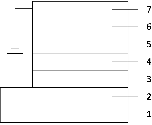
[0042] Such as figure 1 As shown, in the device structure, the anode layer 2 is ITO, the hole transport material 3 is TPAF, and the light-emitting layer 4 is TPAF:B3PYMPM:Ir(ppy) 2 acac(2.00:4.50:0.57), the electron transport layer 5 is B3PYMPM, the electron injection layer 6 is LiF, and the cathode layer 7 is Al. The entire device structure is described as:

[0043] Glass substrate / ITO(150nm) / TPAF(15nm) / TPAF:B3PYMPM:Ir(ppy) 2 The preparation method of acac(2.00:4.50:0.57, 30nm) / B3PYMPM(45nm) / LiF(0.8nm) / Al(80nm) is as follows:

[0044] ①Use detergent, ethanol solution and deionized water to ultrasonically clean the transparent conductive substrate ITO glass, and dry it with dry nitrogen after cleaning. Wherein the ITO film on the glass substrate is used as the anode layer of the device, the square resistance of the ITO film is 15Ω / sq, and the film thickness is 150nm.

[0045] ② Move the dried substrate into a UV-ozone treatment apparatus, and treat the ITO glass with UV-oz...

Embodiment 2

[0051] Such as figure 1 As shown, in the device structure, the anode layer 2 is ITO, the hole transport material 3 is TPAF, and the light-emitting layer 4 is TPAF:B3PYMPM:Ir(MDQ) 2 acac(2.00:4.50:0.13), the electron transport layer 5 is B3PYMPM, the electron injection layer 6 is LiF, and the cathode layer 7 is Al. The entire device structure is described as:

[0052] Glass substrate / ITO / TPAF(40nm) / TPAF:B3PYMPM:Ir(MDQ) 2 acac(2.00:4.50:0.13,30nm) / B3PYMPM(45nm) / LiF(0.8nm) / Al(80nm)

[0053] The fabrication process of the device is similar to that of Example 1.

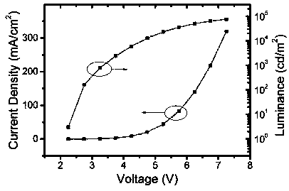
[0054] from Figure 4 , Figure 5 And the test results can be seen in Table 1.

Embodiment 3

[0056] Such as figure 1 As shown, in the device structure, the anode layer 2 is ITO, the hole transport material 3 is TPAF, the light emitting layer 4 is TPAF:B3PYMPM:DCJTB (2.00:4.50:0.06), the electron transport layer 5 is B3PYMPM, and the electron injection layer 6 is LiF , the cathode layer 7 is Al. The entire device structure is described as:

[0057] Glass substrate / ITO / TPAF(40nm) / TPAF:B3PYMPM:DCJTB(2.00:4.50:0.06,30nm) / B3PYMPM(45nm) / LiF(0.8nm) / Al(80nm)

[0058] The fabrication process of the device is similar to that of Example 1.

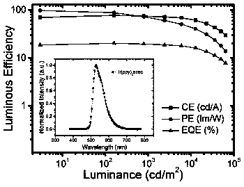
[0059] from Image 6 , Figure 7 And the test results can be seen in Table 1.

[0060] Table 1: Test results of organic electroluminescent devices in Examples 1-3

[0061]


PUM


Abstract

The invention discloses an organic electroluminescent device based on an exciplex and a preparation method thereof. The organic electroluminescent device comprises: a substrate, an anode layer positioned on the surface of the substrate, a functional layer positioned on the anode layer, a cathode layer formed on the functional layer, the functional layer including a hole transport layer, a light-emitting layer, an electron transport Layer and electron injection layer, the light-emitting layer is composed of hole transport material, electron transport material and fluorescent light-emitting material or phosphorescent light-emitting material, and the hole transport material and electron transport material form an exciplex. The exciplex formed by the hole transport material and the electron transport material is the host material of the light emitting layer. Fluorescence light emitting material or phosphorescent light emitting material is a fluorescent light emitting material or phosphorescent light emitting material whose luminescence peak is greater than or equal to the exciplex luminescence peak. The device structure can reduce the carrier injection barrier and reduce the turn-on voltage. The organic electroluminescent device of the invention has simple structure, low driving voltage and high efficiency.

Description

technical field [0001] The invention relates to the field of organic photoelectric technology, in particular to an exciplex-based organic electroluminescent device and a preparation method thereof. Background technique [0002] Organic light-emitting devices (OLEDs) is a new type of display technology, which is widely used in various fields of production and life, such as flat panel display, solid-state lighting, flexible transparent display, etc., and can meet the current world's demand for saving Energy, low-carbon environmental protection and green living requirements. [0003] In 1987, C.W.Tang and Van Slyke of Kodak Corporation of the United States successfully developed a two-layer organic small molecule electroluminescence device. The green OLED can achieve an external quantum efficiency of 1% with a low driving voltage of less than 10V, a power efficiency of 1.5lm / W, and a luminous brightness of up to 1000cd / m2. Then in 1990, R H Friend and others from the Universi...

Claims


Application Information

Patent Timeline
Patent Type & Authority Patents(China)
IPC IPC(8): H01L51/50H01L51/54H01L51/56
CPCH10K85/111H10K50/15H10K50/00H10K71/00
Inventor 张晓宏陶斯禄郑才俊
Owner SUZHOU UNIV
Why Eureka
Try Eureka