
Ultra-thick copper printed board and solder resisting processing method

An ultra-thick copper and printed board technology, applied in printed circuit manufacturing, printed circuits, printed circuits, etc., can solve problems such as difficult operation, unsuitable processing, screen printing alignment problems, etc., to avoid voids and air bubbles Produce, improve the efficiency of solder mask processing, improve the effect of solder mask quality

Inactive Publication Date: 2017-03-22
WUXI SHENNAN CIRCUITS CO LTD
View PDF6 Cites 11 Cited by
  • Summary
  • Abstract
  • Description
  • Claims
  • Application Information

AI Technical Summary

Problems solved by technology

However, with this method, the following problems still exist when printing resin: 1. Because the circuit gap is too deep, it is difficult for the printed resin to fully fill the circuit gap, especially the bottom, and there is a problem of bottom suspension; 2. When printing resin, a large amount of Bubbles, which cannot be completely released, will seriously affect the printing quality; 3. There is an alignment problem in screen printing, and the operation is difficult; 4. This process uses a printing process, which is not suitable for processing ultra-thick copper printing with a thickness of more than 10OZ on the surface layer board

Method used


Image

  • Ultra-thick copper printed board and solder resisting processing method
  • Ultra-thick copper printed board and solder resisting processing method
  • Ultra-thick copper printed board and solder resisting processing method

Examples


Embodiment 1

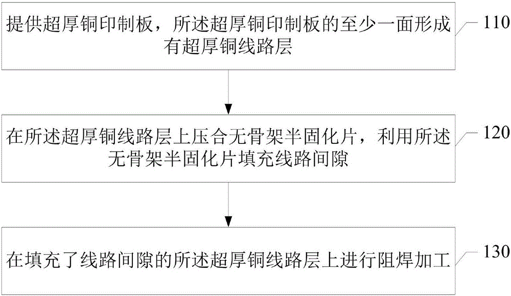
[0024] Please refer to figure 1 , an embodiment of the present invention provides a solder resist processing method for an ultra-thick copper printed board, the method may include:

[0025] 110. Provide an ultra-thick copper printed board, at least one side of the ultra-thick copper printed board is formed with an ultra-thick copper circuit layer, and the thickness of the ultra-thick copper circuit layer is not less than 10OZ.

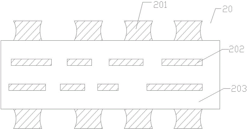
[0026] In the embodiment of the present invention, the ultra-thick copper printed board refers to a printed board with an ultra-thick copper foil layer on one or both sides. Such as Figure 2a As shown, it is a structural schematic diagram of an ultra-thick copper printed board 20 that has completed the outer layer pattern processing. The ultra-thick copper printed board 20 includes: an ultra-thick copper circuit layer 201 located on one or both sides, and a layer located on the inner layer or multiple inner wiring layers 202, and an insulating layer...

Embodiment 2

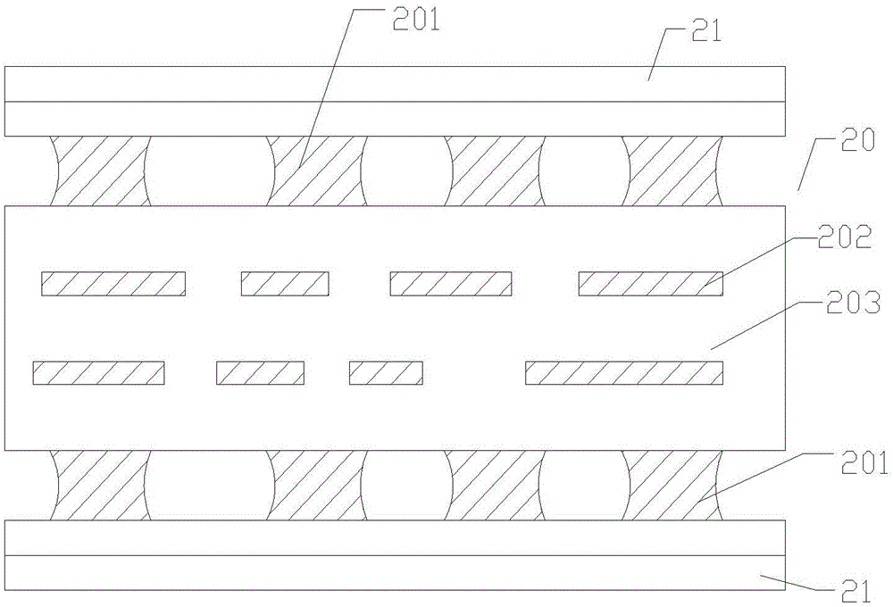
[0041] Please refer to Figure 2e , the embodiment of the present invention provides an ultra-thick copper printed board 20, at least one side of the ultra-thick copper printed board 20 is formed with an ultra-thick copper circuit layer 201, and the thickness of the ultra-thick copper circuit layer 201 is not less than 10OZ ; The circuit gap of the ultra-thick copper circuit layer 201 is filled with a skeleton-free prepreg 21 ; the solder resist ink 22 is set on the ultra-thick copper circuit layer 201 filled with circuit gaps.

[0042] Optionally, the thickness of the ultra-thick copper circuit layer 201 is not less than 15 OZ.

[0043] Above, the embodiment of the present invention discloses an ultra-thick copper printed board, which can be prepared by the method disclosed in Embodiment 1. For a more detailed description of the ultra-thick copper printed board, please Refer to the description in Example 1.

[0044] It can be seen from the above that in some feasible embodi...


PUM


Abstract

The invention discloses an ultra-thick copper printed board and a solder resisting processing method. With the solder resisting processing method adopted, solder resisting processing difficulties of an ultra-thick copper printed board can be eliminated. The method includes the following steps that: an ultra-thick copper printed board is provided, and an ultra-thick copper circuit layer is formed at least one side of the ultra-thick copper printed board, and the thickness of the ultra-thick copper circuit layer is not smaller than 10OZ; frameless prepregs are pressed onto the ultra-thick copper circuit layer, and the frameless prepregs are used to fill line gaps; and solder resisting processing is performed on the line gap-filled ultra-thick copper circuit layer. The invention also provides a corresponding ultra-thick copper printed board.

Description

[0001] This application claims the priority of the Chinese patent application submitted to the China Patent Office on July 22, 2016, the application number is 201610586449.X, and the invention title is "An ultra-thick copper printed board and its solder resist processing method". The entire contents are incorporated by reference in this application. technical field [0002] The invention relates to the technical field of printed circuit board production, in particular to an ultra-thick copper printed board and a welding resistance processing method thereof. Background technique [0003] Printed Circuit Board (PCB), also known as printed circuit board, referred to as circuit board or printed board, is a provider of electrical connections for electronic components. Usually, printed boards need to be processed with solder resist, and a layer of solder resist material is used to play the role of solder resist insulation and prevent circuit oxidation. [0004] With the developme...

Claims


Application Information

Patent Timeline
IPC IPC(8): H05K3/28H05K1/02
CPCH05K3/287H05K1/02H05K2201/09872H05K2203/1377
Inventor 万川郑少康董晋
Owner WUXI SHENNAN CIRCUITS CO LTD
Learn More