
Method for detecting photoelectric current signal of photoelectric conversion material via conductive atomic force microscope

An atomic force microscope and photoelectric conversion material technology, which is applied in the field of signal detection, can solve the problems of difficulty in distinguishing current amplifiers, material temperature rise, photoelectric conversion material damage, etc., and achieves the effect of suppressing useless noise and improving detection signal-to-noise ratio.

Active Publication Date: 2017-03-29
宁波新材料测试评价中心有限公司
View PDF5 Cites 6 Cited by
  • Summary
  • Abstract
  • Description
  • Claims
  • Application Information

AI Technical Summary

Problems solved by technology

[0005] However, limited by the resolution of the current amplifier, for most materials with photoelectric conversion effect, the photocurrent signal generated after irradiation with light intensity is generally very weak, and it is difficult to distinguish it by the current amplifier, and often requires a strong light intensity to generate enough Large photocurrent signals that can be resolved by the current amplifier, and strong light intensity will cause the temperature of the material to rise, increase the thermal drift and thermal noise of the test, and may even cause damage to the photoelectric conversion material, affecting the accuracy of the test results

Method used


Image

  • Method for detecting photoelectric current signal of photoelectric conversion material via conductive atomic force microscope
  • Method for detecting photoelectric current signal of photoelectric conversion material via conductive atomic force microscope
  • Method for detecting photoelectric current signal of photoelectric conversion material via conductive atomic force microscope

Examples


Embodiment 1

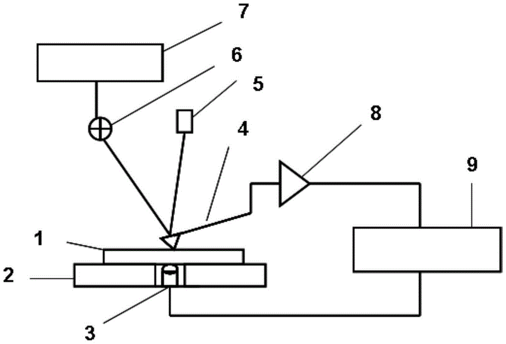
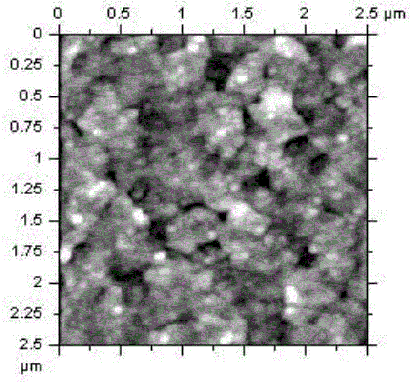
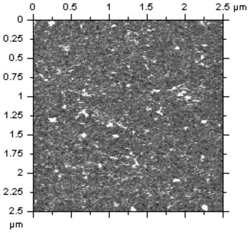
[0028] In this embodiment, the sample is an ITO / P3HT:PCBM film sample with a photoelectric conversion effect, and the surface morphology and photocurrent distribution of the sample are tested by a conductive atomic force microscope.

[0029] The structure diagram of the test platform is as follows: figure 1 As shown, it includes a microscopic topography detection part and a photocurrent signal detection part.

[0030] The microscopic morphology detection process is as follows: the sample 1 is placed on the sample stage 2 of the atomic force microscope micromirror, and the tip of the conductive probe 4 forms a stable contact with the sample. The light source of the laser 5 is incident on the surface of the probe 4 and reflected to the four-quadrant photodetector 6 . The four-quadrant photodetector 6 converts the optical signal into an electrical signal and inputs it to the controller 7 of the atomic force microscope.

[0031] The photocurrent signal detection process is as fo...


PUM


Abstract

The invention provides a method for detecting a photoelectric current signal of a photoelectric conversion material via a conductive atomic force microscope. A lock-in amplifier is used, the lock-in amplifier provides an alternating driving voltage so that a light source is driven to emit light to irradiate a material sample, the sample generates an optical current due to a photoelectric conversion effect, a conductive probe makes contact with the sample to detect the photoelectric current signal and transmits the photoelectric current signal to a current amplifier to obtain a current amplification signal, and the current amplification signal is then input to the lock-in amplifier. Thus, the frequency of a reference signal of lock-in amplification is the same with that of the driving voltage, lock-in amplification of the photoelectric current signal is realized, and the sensitivity and signal to noise ratio of photoelectric current detection are improved.

Description

technical field [0001] The invention belongs to the technical field of signal detection, and in particular relates to a method for detecting photocurrent signals of photoelectric conversion materials by using a conductive atomic force microscope. Background technique [0002] The research on organic solar cells began in the 1970s. Compared with traditional solar cells, organic solar cells have the advantages of designable molecular structure, light material weight, simple production process, low manufacturing cost, good processing performance, and rollability. Therefore, it has received extensive attention in the field of solar cells with the development direction of improving battery performance, reducing production costs, and reducing environmental pollution. [0003] Theoretical studies have shown that the nanostructure of the active layer with photoelectric conversion effect in organic solar cells (that is, the material of the active layer is a photoelectric conversion m...

Claims


Application Information

Patent Timeline
IPC IPC(8): G01Q60/24
Inventor 魏艳萍卢焕明魏安祥陈国新李勇
Owner 宁波新材料测试评价中心有限公司
Learn More