Manufacturing method of nanocrystalline common-mode inductor

A common mode inductance and manufacturing method technology, applied in the field of inductance, can solve the problems of large volume, difficult to balance inductance, small volume, etc.

Active Publication Date: 2017-04-05
DONGGUAN DAZHONG ELECTRONICS
View PDF5 Cites 14 Cited by
  • Summary
  • Abstract
  • Description
  • Claims
  • Application Information

AI Technical Summary

Problems solved by technology

[0002] With the trend of technological development, the common mode inductors in electronic components are changing towards miniaturization and light weight. However, it is difficult to achieve a balance between miniaturization and inductance in the existing technology. Inductance, its volume is relatively large, and the inductance with small inductance, its volume is correspondingly small, it is difficult to achieve large inductance, but its volume is small

Method used


Image

  • Manufacturing method of nanocrystalline common-mode inductor

Examples


Embodiment Construction

[0037] The present invention is further described in conjunction with the following examples.

[0038] A method for manufacturing a nanocrystalline common-mode inductor in this embodiment includes the following steps:

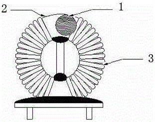
[0039] Step 1: Install a core mold with a diameter of 22mm on the amorphous automatic winding machine, and wind the 13mm long iron-based nanocrystalline strip into a nanocrystalline magnetic ring with an outer diameter of 38mm, an inner diameter of 22mm, and a height of 13mm 1.

[0040] Then, detect the tightness of the amorphous magnetic ring: the external force pushes the nanocrystalline magnetic ring 1 from the direction perpendicular to the bandwidth of the nanocrystalline magnetic ring 1

[0041] Compression deformation, after the external force is removed, the height dimension of the magnetic ring in the direction of the force can be restored to 80% greater than that before the external force is not applied. This step can eliminate the internal stress of...


PUM

PropertyMeasurementUnit
heightaaaaaaaaaa
thermal resistanceaaaaaaaaaa
diameteraaaaaaaaaa

Abstract

The invention discloses a manufacturing method of a nanocrystalline common-mode inductor, and relates to the technical field of inductors. The method comprises the steps that a nanocrystalline strip is wound into a nanocrystalline magnetic ring with the outer diameter of 38 mm, the inner diameter of 22 mm and the height of 13 mm; the nanocrystalline magnetic ring is put into a vacuum annealing furnace to be subjected to heat treatment; the nanocrystalline magnetic ring obtained after heat treatment is cured and aged with epoxy resin; the cured and aged nanocrystalline magnetic ring is contained in a protection box; coils of two windings are evenly made on the two sides of the protection box of the nanocrystalline magnetic ring through two varnished wires, and then manufacture of the nanocrystalline common-mode inductor is completed. By means of the specially-set heat treatment method, the nanocrystalline common-mode inductor with the inductance larger than 15 mH, the outer size smaller than 48 mm and the thickness smaller than 28 mm can be manufactured, and the purposes of being high in inductance value and small in size are achieved.

Description

technical field [0001] The invention relates to the technical field of inductors, in particular to a method for manufacturing a nanocrystalline common-mode inductor. Background technique [0002] With the trend of technological development, the common-mode inductors in electronic components are changing towards miniaturization and light weight. However, it is difficult to achieve a balance between miniaturization and inductance in the existing technology. Inductors have relatively large volumes, and inductors with small inductances have relatively small volumes. It is difficult to achieve large inductances with small volumes. Contents of the invention [0003] The object of the present invention is to avoid the deficiencies in the prior art and provide a method for manufacturing a nanocrystalline common-mode inductor with an operating current of 15A, an inductance greater than 15mH, an outer dimension less than 48mm, and a thickness less than 28mm. [0004] The object of ...

Claims


Application Information

Patent Timeline
Patent Type & Authority Applications(China)
IPC IPC(8): H01F41/02
CPCH01F41/0213
Inventor 梁文超李正中
Owner DONGGUAN DAZHONG ELECTRONICS
Why Eureka
Try Eureka