Sensing Circuit Used For Non-volatile Memory And Non-volatile Memory

A sensing circuit and voltage technology, applied in information storage, static memory, read-only memory, etc., can solve problems such as the influence of accuracy of electrical characteristics, the difference of jump points, etc., and achieve the effect of accurate data value and accurate sensing

Active Publication Date: 2017-04-12
POWERCHIP SEMICON MFG CORP
View PDF9 Cites 6 Cited by
  • Summary
  • Abstract
  • Description
  • Claims
  • Application Information

AI Technical Summary

Problems solved by technology

Also, if the P-channel MOS transistors and N-channel MOS transistors are arranged with a slight deviation, the deviation of the trip point may differ by more than 10% in the worst case.
In this way, variations in the electrical characteristics of MOS transistors will have a large impact on the accuracy of sensing in further miniaturized flash memories.

Method used


Image

  • Sensing Circuit Used For Non-volatile Memory And Non-volatile Memory
  • Sensing Circuit Used For Non-volatile Memory And Non-volatile Memory
  • Sensing Circuit Used For Non-volatile Memory And Non-volatile Memory

Examples


Embodiment 1

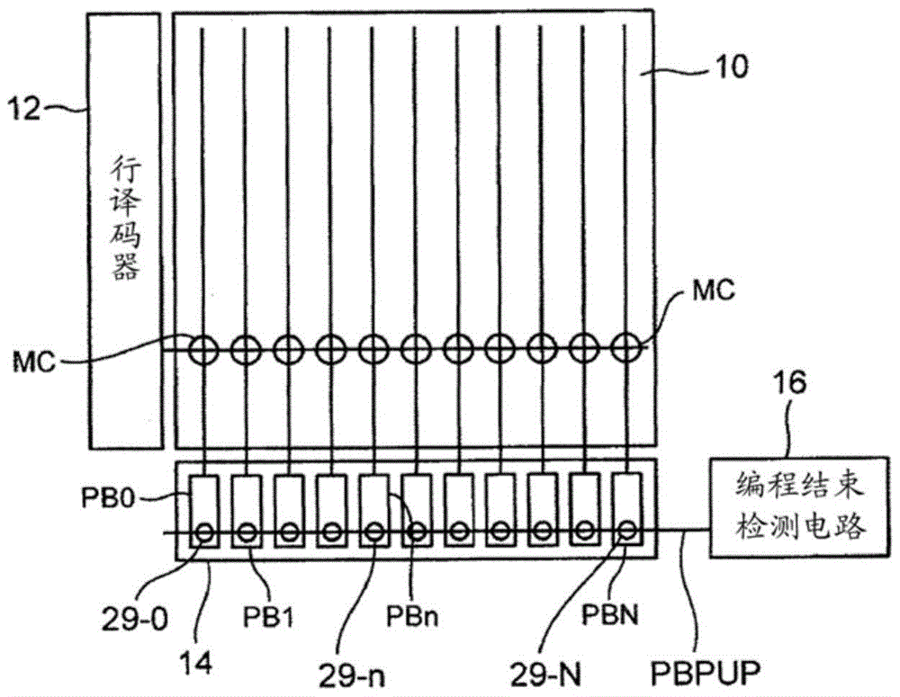
[0175] Figure 7 It is a circuit diagram showing a configuration example of the sensing circuit 30A and the page buffer PBn used in the NAND flash EEPROM of the first embodiment. Figure 7 In the embodiment 1, the sensing circuit 30A is provided corresponding to each page buffer PBn, and is provided between the nodes SNS and SLS1 of the page buffer PBn and the signal line B, and has a stacked gate type An N-channel MOS transistor N1 and two N-channel MOS transistors N2 and N3 each serving as a switch element are configured.

[0176] The control gate of the MOS transistor N1 is connected to the node SNS (sensing node of the page buffer PBn), the floating gate of the MOS transistor N1 is connected to the source of the MOS transistor N2, and the source of the MOS transistor N1 is connected to the signal line B. The drain of the MOS transistor N1 is connected to the source of the MOS transistor N3 and the drain of the MOS transistor N2. And, to the gate of the MOS transistor N2,...

Embodiment 2

[0192] Figure 9 It is a circuit diagram showing a configuration example of the sensing circuit 30B and the page buffer PBn used in the NAND flash EEPROM of the second embodiment. The sensing circuit 30B of Embodiment 2 is used for data programming and verification processing (including when the node voltage SLR1 is low level and programming is performed, and when the node voltage SLR1 is high level but not performed) in addition to data readout. programming case) sensing circuitry, with Figure 7 Compared with the sensing circuit 30A of the first embodiment, the following points are different.

[0193] (1) In addition to the MOS transistors N1 and N2, the sensing circuit 30B further includes an N-channel MOS transistor N5 and an N-channel MOS transistor N4. The N-channel MOS transistor N5 is a switch connected to the signal line A and the node SLS1. component, the N-channel MOS transistor N4 is a switch component that is turned on / off based on the verification judgment swit...

Embodiment 2-1

[0198] Figure 10 is expressed by Figure 9 Flowchart of the data programming and verifying process of Embodiment 2-1 (programming is performed when SLR1=Low and SLR1=0V, SLS1=VDD) executed by the sensing circuit 30B and page buffer PBn of the . Figure 10 Data programming and verification processing and Figure 8 Compared with the data read processing of , the following points are different. In addition, in Figure 10 In each treatment, the bottom line is used to indicate the relationship with Figure 8 The difference in the corresponding processing of , and the difference from the previous corresponding processing is also indicated below with an underline.

[0199] (1) replace Figure 8 The processing of steps S1 to S4 includes the processing of steps S21 and S22.

[0200] (2) replace Figure 8 Steps S8 and S12 of the step S8A and S12A respectively include the processing of steps S8A and S12A.

[0201] (3) After the processing of step S13, execute Figure 11 The pr...


PUM


Abstract

The present invention relates to a sensing circuit used for a non-volatile memory and the non-volatile memory. The sensing circuit is arranged in a page buffer with a latch and senses the data, and the latch saves the data temporarily when writing in or reading out data from a storage unit of the non-volatile memory. The sensing circuit comprises a first switch assembly and a stack gate type control assembly which are connected in series between a first signal line and the first terminal of the latch; a second switch assembly connected between the first switch assembly and the stack gate type control assembly. Before the first switch assembly is conducted to sense by a sensing enabling signal, the voltage of a floating gate of the stack gate type control assembly is set as the voltage value which is the sum of a limit value voltage of the floating gate of the stack gate type control assembly and a specified voltage, and then the data of the storage unit is sensed.

Description

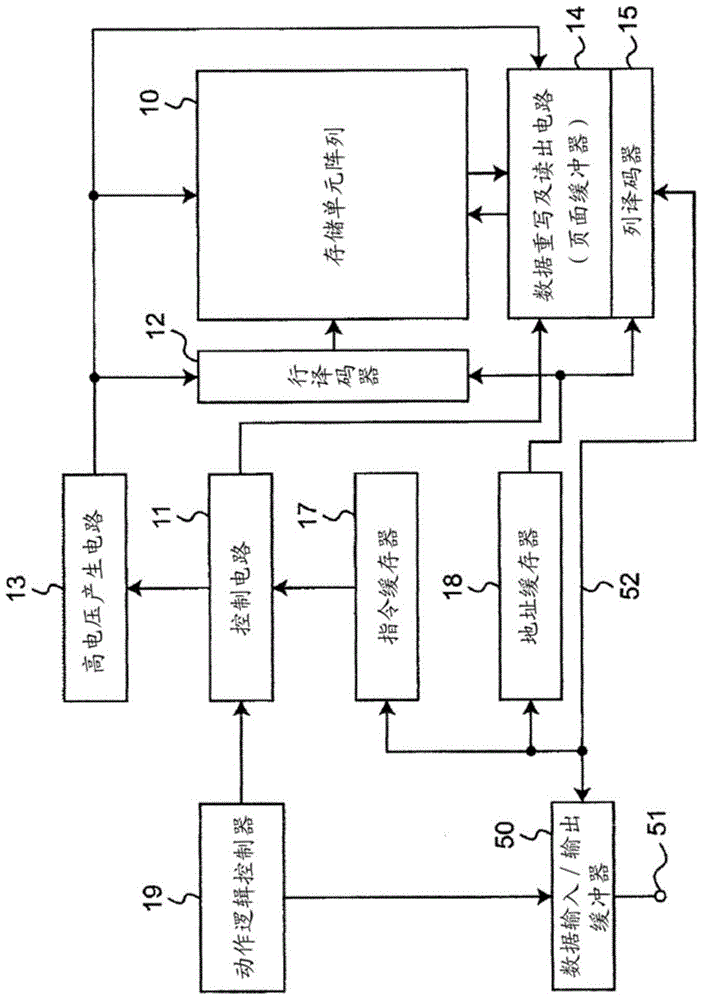
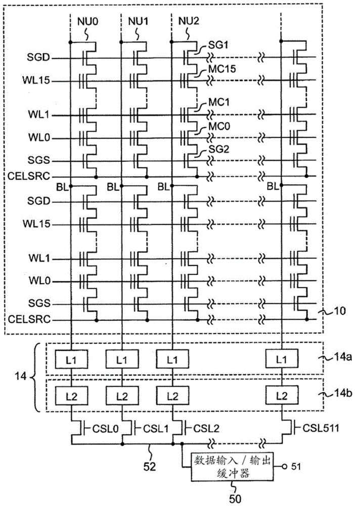
technical field [0001] The present invention relates to a sensing device (Electrically Erasable Programmable Read-Only Memory (Electrically Erasable Programmable Read-Only Memory, EEPROM)) which is used for electrically rewritable non-volatile semiconductor storage devices such as flash memory (flash memory) circuits and non-volatile memory devices. Background technique [0002] There is known a NAND type nonvolatile semiconductor storage device in which a plurality of memory cell transistors (memory cell transistors) are connected in series between a bit line (bit line) and a source line (source line) (hereinafter It is called a memory cell) to form a NAND string (string), thereby achieving high integration (for example, refer to Patent Document 1). [0003] Figure 1A It is a block diagram showing the overall configuration of a conventional NAND-type flash EEPROM. and, Figure 1B yes means Figure 1A A circuit diagram of the configuration of the memory cell array (memor...

Claims


Application Information

Patent Timeline
IPC IPC(8): G11C16/26G11C16/10
CPCG11C16/10G11C16/26
Inventor 小川晓
Owner POWERCHIP SEMICON MFG CORP
Why Eureka
Try Eureka