Capacitance touch display device

A technology of capacitive touch and display devices, which is applied in the direction of electrical digital data processing, instruments, and input/output processes of data processing, etc., can solve the problems of reduced strength, inability to effectively improve the signal-to-noise ratio, and capacitive touch display. Device performance limitations and other issues, to achieve the effect of reduced intensity, improved signal-to-noise ratio, and accurate sensing

Inactive Publication Date: 2013-04-17
RAYDIUM SEMICON
View PDF4 Cites 6 Cited by
  • Summary
  • Abstract
  • Description
  • Claims
  • Application Information

AI Technical Summary

Problems solved by technology

However, since the sensing voltage V sensed by adjacent sensing lines X0 and X1 at the same time S0 with V S1 are respectively the driving voltage V provided by nodes N00 and N10 coupled from the same driving line Y0 D0 , that is, the sensing voltage V sensed by adjacent sensing electrodes X0 and X1 S0 with V S1 have the same phase, therefore, although the sensing circuit SC will differentially input the sensing voltage V of adjacent sensing lines X0 and X1 S0 with V S1 The influence of noise can be reduced after subtraction, but the strength of signals with the same phase will also be reduced after subtraction, so the signal-to-noise ratio cannot be effectively improved significantly, resulting in the limitation of the performance of the capacitive touch display device

Method used


Image

  • Capacitance touch display device
  • Capacitance touch display device
  • Capacitance touch display device

Examples


Embodiment Construction

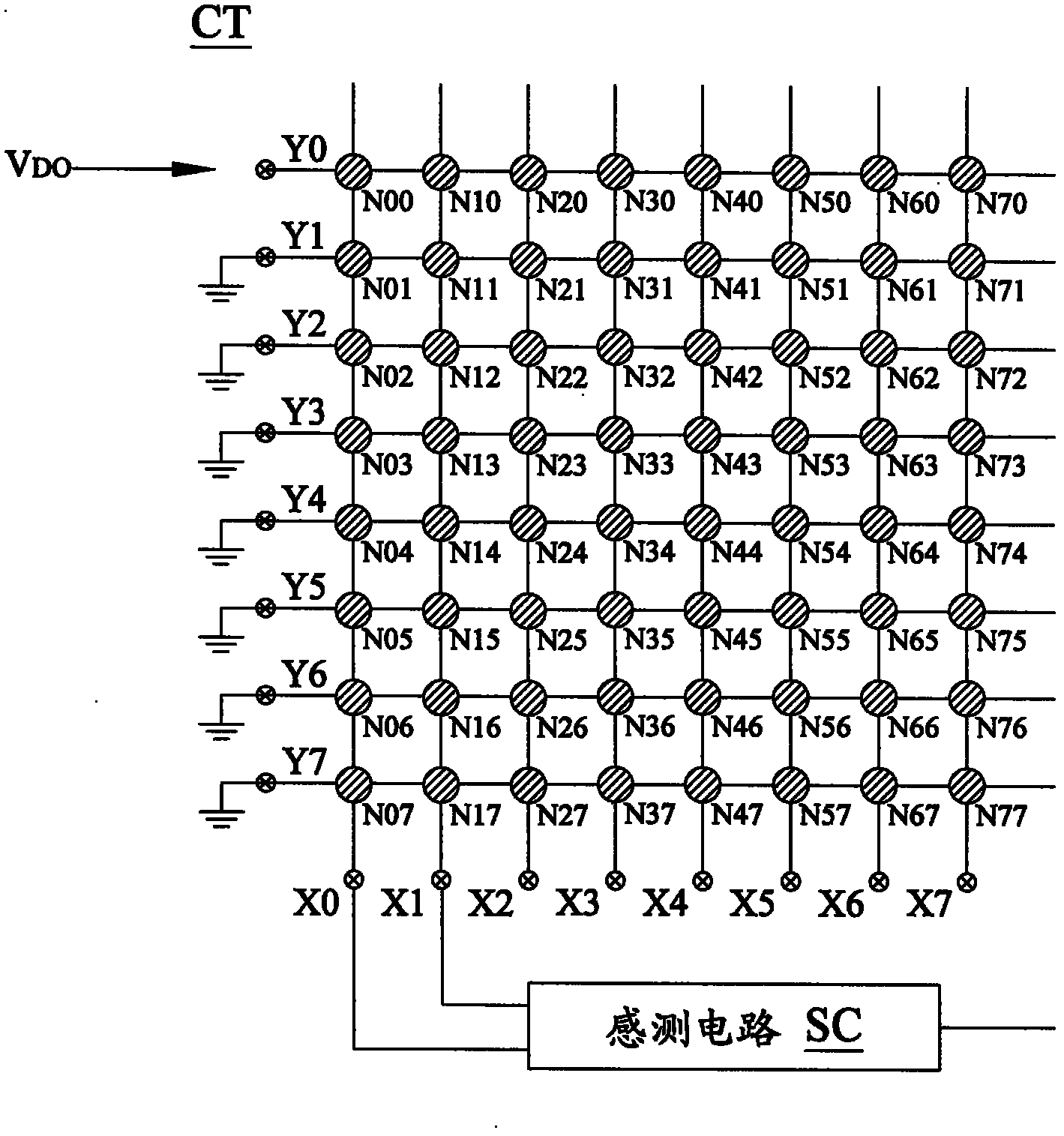
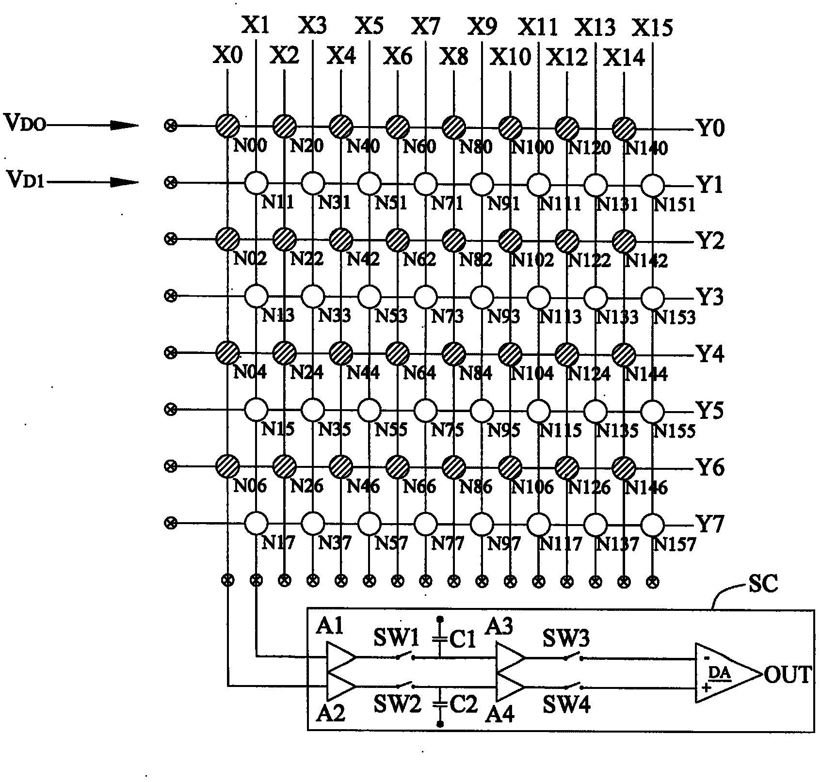
[0034] A specific embodiment according to the present invention is a capacitive touch display device. In this embodiment, the capacitive touch display device at least includes a capacitive touch panel and a capacitive touch sensor, and the capacitive touch sensor can adopt mutual capacitance type touch sensing The touch points formed on the capacitive touch panel can be sensed by the method, but not limited thereto. Please refer to image 3 , image 3 It is a schematic diagram showing the nodes of the driving lines (electrodes) and the sensing lines (electrodes) of the capacitive touch display device of the present invention arranged alternately.

[0035] Such as image 3 As shown, the driving lines Y0 ˜ Y7 and the sensing lines X0 ˜ X15 form a total of 64 nodes N00 , N20 , . . . , N11 , N31 , . Compared to figure 2 existing technology, image 3 The number of nodes and the number of driving lines are the same as figure 2 as shown, but image 3 The number of sensing l...


PUM


Abstract

The invention provides a capacitance touch display device including a capacitance touch control panel and a capacitance touch con trol sensor. The capacitance touch control sensor includes a plurality of driving lines, a plurality of sensing lines and a sensing circuit. At a certain time point, the first driving line and the second driving line arranged in alternate permutation are used for inputting first driving voltage and second driving voltage with different phase and voltage. A first node is form by overlapping the first sensing line with the first driving line and does not overlap with the second driving line. The second sensing line overlaps with the second driving line, so that a second node is formed and does not overlap with the first driving line. A first mutually-inducting capacitance and a second mutually-inducting capacitance are formed by coupling the first node with the second node, and a first sensing voltage and a second sensing voltage are formed and are output by the first sensing line and the second sensing line. A sensing voltage value of a sensing circuit is obtained by subtracting the first sensing voltage and the second sensing voltage.

Description

technical field [0001] The present invention is related to liquid crystal displays; specifically, the present invention relates to a capacitive touch display device, which uses an interlaced electrode arrangement to make the sensing voltages sensed by adjacent sensing lines at the same time It can come from different driving lines providing different driving voltages respectively, so as to improve its Signal-Noise Ratio (SNR). Background technique [0002] With the rapid development of technology, thin film transistor liquid crystal displays (TFT LCDs) have gradually replaced traditional displays, and have been widely used in various electronic products such as TVs, flat panel displays, mobile phones, tablet computers, and projectors. For a TFT-LCD with touch function, the touch sensor is one of the important modules, and its performance directly affects the overall performance of the LCD. [0003] Such as figure 1 As shown, a capacitive touch sensor generally used for sen...

Claims


Application Information

Patent Timeline
Patent Type & Authority Applications(China)
IPC IPC(8): G06F3/044
Inventor 詹前煜左克扬
Owner RAYDIUM SEMICON
Why Eureka
Try Eureka