Detector for positron emission imaging equipment, and positron emission imaging equipment

A technology for positron emission and imaging equipment, which is applied in radiological diagnostic instruments, radiation measurement, X/γ/cosmic radiation measurement, etc., and can solve problems such as loss of photon signals, impact on positioning accuracy, and decline in crystal filling rate , to achieve the effect of low mechanical design difficulty, high positioning accuracy and weak edge effect

Inactive Publication Date: 2017-04-19
WUHAN ZHONGPAI TECH CO LTD
View PDF6 Cites 21 Cited by
  • Summary
  • Abstract
  • Description
  • Claims
  • Application Information

AI Technical Summary

Problems solved by technology

(1) Since the detectors are spliced ​​together, there is a certain position error in the entire detector system, which has a certain impact on the positioning accuracy of gamma photon pairs, thereby reducing the spatial resolution of the positron emission imaging device
(2) Affected by factors such as the gap between the detectors and the wall thickness of the packaging box, the crystal filling rate will decrease, resulting in the loss of some photon signals, which will reduce the sensitivity of the positron emission imaging equipment
(4) Since the detectors need to be spliced ​​together through a complex mechanical structure, problems such as the support, coordination, and alignment of the detectors need to be solved when designing the mechanical system, resulting in the mechanical design of the positron emission imaging equipment. Difficult and costly

Method used


Image

  • Detector for positron emission imaging equipment, and positron emission imaging equipment
  • Detector for positron emission imaging equipment, and positron emission imaging equipment
  • Detector for positron emission imaging equipment, and positron emission imaging equipment

Examples


Embodiment Construction

[0017] In the following description, numerous details are provided in order to provide a thorough understanding of the invention. However, it will be appreciated by those skilled in the art that the following description relates only to preferred embodiments of the invention and that the invention may be practiced without one or more of these details. In addition, in order to avoid confusion with the present invention, some technical features known in the art are not described.

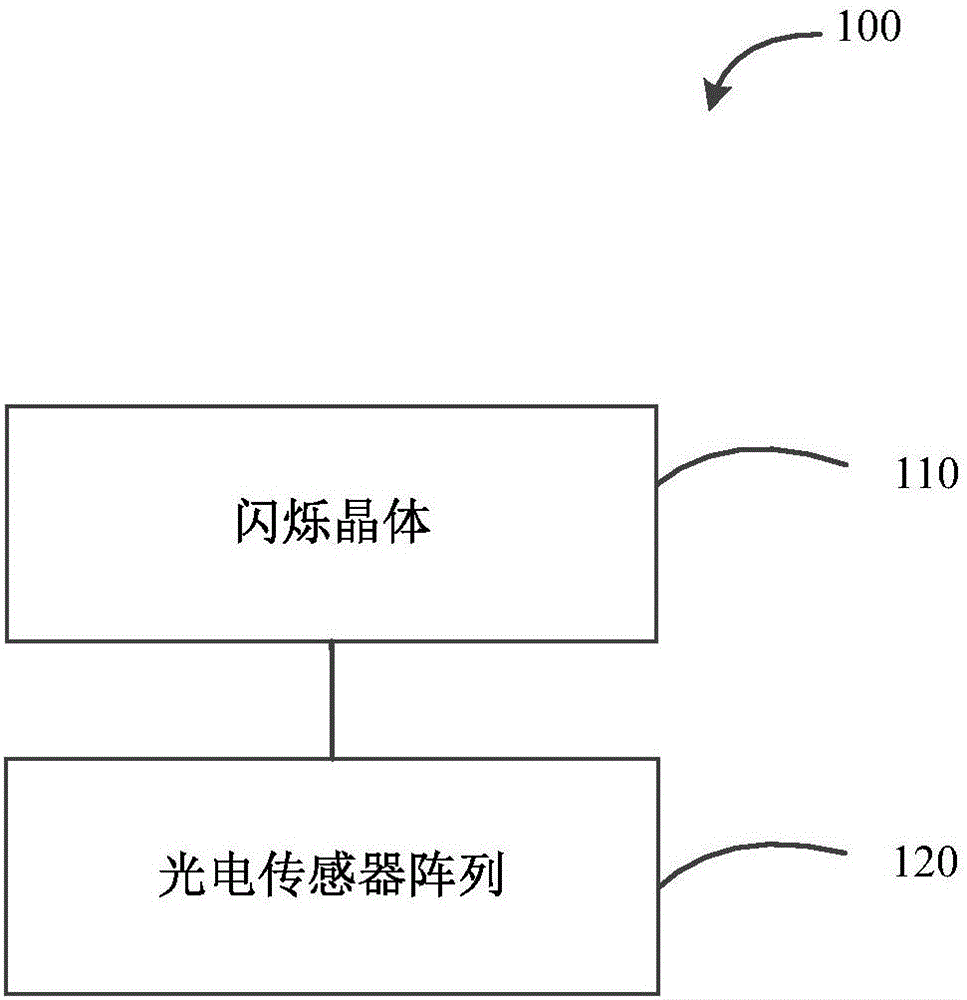
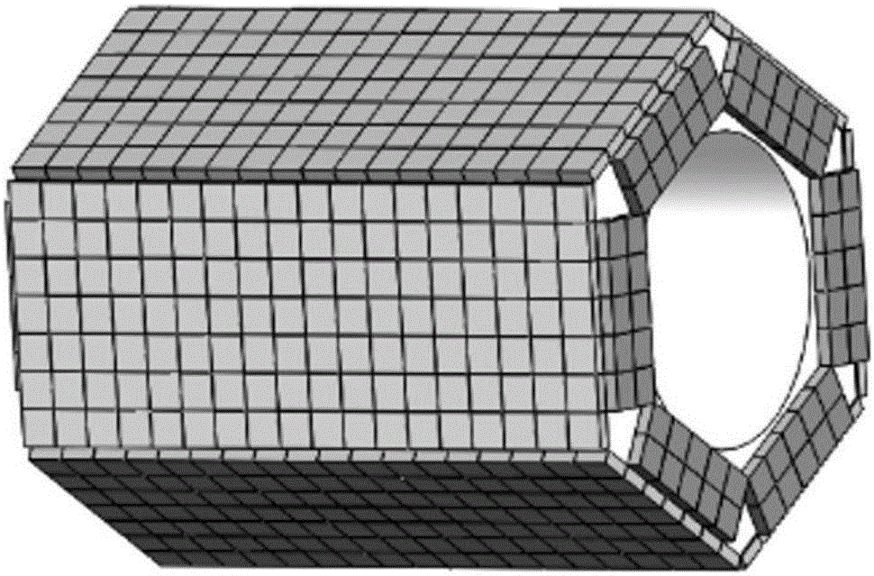
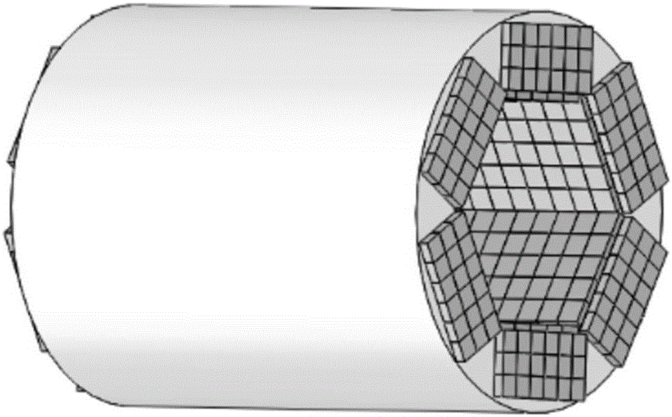
[0018] In order to solve the above problems, the present invention proposes a detector for a positron emission imaging device and a positron emission imaging device. According to the embodiments of the present invention, the integrated scintillation crystal and photosensor array adapted to form a detector can solve the problem caused by splicing detectors in traditional positron emission imaging equipment.

[0019] figure 1 A schematic block diagram of a detector 100 for a positron emission imaging ...


PUM


Abstract

The invention provides a detector for positron emission imaging equipment, and positron emission imaging equipment. The detector includes a scintillation crystal and at least one photoelectric sensor array, wherein the scintillation crystal is an integrated scintillation crystal, and is provided with a through hole; the through hole is used for accommodating an object waiting for imaging; the photoelectric sensor array is coupled with the scintillation crystal, and is used for detecting a visible photon which is generated when a gamma photon and the scintillation crystal react; and the gamma photon is generated through positron annihilation effect which occurs in the object waiting for imaging. The detector for positron emission imaging equipment enables the positron emission imaging equipment using the detector to be high in positioning accuracy of the gamma photon, to be high in sensitivity, to be weak in edge effect and to be low in mechanical design difficulty.

Description

technical field [0001] The invention relates to the field of positron emission imaging, in particular to a detector for a positron emission imaging device and the positron emission imaging device. Background technique [0002] The full name of positron emission imaging is Positron Emission Computed Tomography (PET). The main means of clinical diagnosis. [0003] In traditional positron emission imaging equipment, a plurality of square detectors (including scintillation crystals, photoelectric sensors, etc.) are generally spliced ​​into a circular or approximately spherical detector system through a mechanical structure to detect gamma photons. Specifically, each scintillation crystal (or scintillation crystal array) of a traditional positron emission imaging device is coupled with a photosensor to form an independent detector, and multiple independent detectors are spliced ​​together through a complex mechanical structure to form a positron A detector system for an emissio...

Claims


Application Information

Patent Timeline
Patent Type & Authority Applications(China)
IPC IPC(8): A61B6/03G01T1/202G01T1/29
CPCA61B6/037A61B6/4258G01T1/202G01T1/2985
Inventor 谢思维黄秋龚政赵指向翁凤花彭旗宇
Owner WUHAN ZHONGPAI TECH CO LTD
Why Eureka
Try Eureka