Microwave chip screening device and screening method therefor

A microwave chip and screening device technology, which is applied in the direction of measuring devices, measuring device shells, and electronic circuit testing, can solve the problems of increased equipment cost, waste, and small force, and achieve good versatility, reduced scrapping, and convenient operation Effect

Active Publication Date: 2017-04-26
WUXI HUACE ELECTRONICS SYST
View PDF4 Cites 2 Cited by
  • Summary
  • Abstract
  • Description
  • Claims
  • Application Information

AI Technical Summary

Problems solved by technology

However, with the development of the industry, there are more and more performance indicators of a single microwave chip. If only the probes are used to test all indicators, the cost of the microwave chip will undoubtedly increase.
Also, the probe method cannot perform low temperature and power resistant screening
In addition, most of the existing temporary packaging carrier methods are to apply elastic pressure to the point contact of the chip pad. Small, not conducive to high-power microwave chip-to-ground contact heat

Method used


Image

  • Microwave chip screening device and screening method therefor
  • Microwave chip screening device and screening method therefor
  • Microwave chip screening device and screening method therefor

Examples


Embodiment Construction

[0033] Specific embodiments of the present invention will be described below.

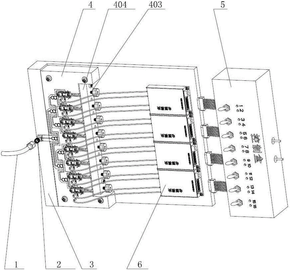
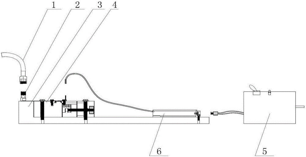
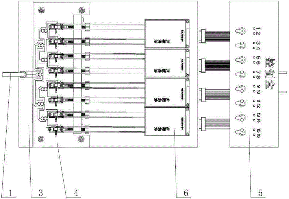
[0034] Such as figure 1 , figure 2 and image 3 As shown, a microwave chip screening device and a screening method thereof include a base 3, on which a clamping tool 4 with a circuit component 2 and a plurality of power supply modules 6 for power-on are respectively arranged on the base 3, and the circuit component 2 and the power supply The signal end and the load end of the module 6 are electrically connected, and a power output port is provided at the tail of the base 3, and the control box 5 is connected to the power output port.

[0035] Such as figure 2 , Figure 4 , Figure 5 and Figure 6 As shown, the specific structure of the clamping tooling 4 is as follows:

[0036] It includes a bottom plate 406 for carrying and positioning chip components 407, and a plurality of limit chute is set on the bottom plate 406, and the slider 401 is slidably arranged in each limit chute, and the sl...


PUM


Abstract

The invention relates to a microwave chip screening device and a screening method therefor. The device comprises a pedestal, a clamping tool equipped with a circuit part and a plurality of power source modules used for power supply are arranged on the pedestal, wherein the circuit part is electrically connected with signal ends and load ends of the power source modules, a power source output port is arranged on a tail part of the pedestal, and a control box is connected with the power source output port. Via the microwave chip screening device and the screening method therefor, lossless testing, high and low temperature screening and power capacity screening of a microwave chip part can be realized; compared with other method, the device is advantageous in that damage-caused scrappage of chips can be lowered; via the device, that all kinds of microwave chip parts are excellent grounding performance and high in applicability can be ensured. The clamping tool installed in the device and the circuit part mounted on the clamping tool can be subjected to fine tuning operation according to size of the microwave chips, and each chip does not need to be redesigned; the microwave chip screening device and the screening method therefor are advantaged by convenience of operation, good universality, low cost and the like.

Description

technical field [0001] The invention relates to the field of microwave chip testing, in particular to a microwave chip screening device and a screening method thereof. Background technique [0002] At present, the existing microwave chip testing methods are probe testing or loading into a temporary package carrier for testing. However, with the development of the industry, there are more and more performance indicators of a single microwave chip. If only probes are used to test all indicators, the cost of microwave chips will undoubtedly be increased. Also, the probe method cannot perform low temperature and power resistant screening. In addition, most of the existing temporary packaging carrier methods are to apply elastic pressure to the point contact of the chip pad. Small, not conducive to high-power microwave chip-to-ground contact heat dissipation. If the method of vacuum absorbing chips is adopted, an external vacuum pipeline is required, which increases the equipm...

Claims


Application Information

Patent Timeline
IPC IPC(8): G01R31/28G01R1/04
CPCG01R1/0425G01R31/2856Y02P70/50
Inventor 程志远魏宪举刘均东薛国锋
Owner WUXI HUACE ELECTRONICS SYST
Why Eureka
Try Eureka