Substrate for testing Seebeck coefficient of semiconductor thin film, preparation and testing method

A technology of Seebeck coefficient and test method, applied in the direction of measuring device, instrument, material thermal development, etc., can solve the problems of damage to the sample to be tested, poor measurement repeatability, limited temperature tolerance of silver paste, etc.

Active Publication Date: 2020-03-13
XIAN TECH UNIV
View PDF6 Cites 0 Cited by
  • Summary
  • Abstract
  • Description
  • Claims
  • Application Information

AI Technical Summary

Problems solved by technology

However, for samples using conductive silver paste as electrodes, due to the limited temperature resistance of silver paste, the electrodes will fail at high temperatures, resulting in inaccurate test results; while using clamp electrodes, the fixture forms point contact with the material. On the one hand, it is easy to Cause damage to the sample to be tested. On the other hand, the difference in contact position will lead to poor measurement repeatability

Method used


Image

  • Substrate for testing Seebeck coefficient of semiconductor thin film, preparation and testing method
  • Substrate for testing Seebeck coefficient of semiconductor thin film, preparation and testing method
  • Substrate for testing Seebeck coefficient of semiconductor thin film, preparation and testing method

Examples


Embodiment

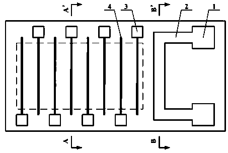
[0036] Embodiment: using polished silicon wafer as substrate, substrate length: 20mm, width: 10mm, thickness 0.2mm; insulating film layer adopts silicon oxide, deposited thickness 1μm; thermal resistance electrode, test electrode and lead wire adopt metallic titanium, thickness 500nm; The resistor is made of metal molybdenum, with a width of 1mm and a thickness of 500nm; the thermal resistance electrode is a square, with a side length of 2mm, and the center distance between two thermal resistance electrodes is 7mm; the test electrode is a square, with a side length of 1mm, a lead length of 7mm, and a line width of 0.1mm. The spacing between adjacent leads is 1.5mm.

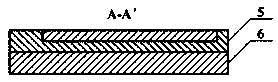
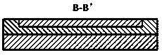
[0037] A method for preparing a substrate for testing the Seebeck coefficient of a semiconductor thin film is (see Figure 5 ): the insulating film layer 5 is deposited on the substrate 6 by thermal evaporation or magnetron sputtering; and then the photoresist is spin-coated on the insulating film layer 5, the spi...


PUM

PropertyMeasurementUnit
thicknessaaaaaaaaaa
thicknessaaaaaaaaaa
thicknessaaaaaaaaaa

Abstract

The invention belongs to the field of semiconductor material measuring equipment, and particularly relates to a substrate for testing a Seebeck coefficient of a semiconductor thin film and preparation and testing methods. After a patterned insulating layer is deposited on a polished substrate, a patterned area is filled with thermal resistor electrodes, a thermal resistor, test electrodes and a lead, and the patterns of the electrodes and the lead are designed according to the Seebeck coefficient test requirements; during test of the Seebeck coefficient of the semiconductor thin film, the measured thin film is deposited in an effective area and covers the lead. A large current power source is connected onto the two thermal resistor electrodes, the temperature of the thermal resistor is controlled by the current magnitude of the power source. When the temperature of the thermal resistor is constant, the temperature difference between temperature measurement points is detected, and the potential difference between the test electrodes is collected to obtain the Seebeck coefficient of the material. When the substrate and the method provided by the invention are used for testing the Seebeck coefficient, the failure of the lead due to high temperature cannot occur, and that a sample is damaged by direct contact between a probe and the thin film to be measured cannot occur either, so that the commercial application of the Seebeck coefficient test equipment for the thin film is promoted.

Description

technical field [0001] The invention belongs to the field of semiconductor material measuring equipment, and in particular relates to a substrate for testing the Seebeck coefficient of a semiconductor thin film and a preparation and testing method. Background technique [0002] The Seebeck effect, also known as the first thermoelectric effect, refers to the phenomenon that an electromotive force is generated due to the temperature difference at the two nodes in a circuit composed of two different conductors or semiconductor materials. This kind of electromotive force is called thermoelectromotive force, the current flowing in the loop is called thermoelectric current, and the ratio of thermoelectromotive force to temperature difference is called Seebeck coefficient. [0003] The Seebeck coefficient is one of the most important performance parameters of semiconductor thermoelectric materials. Accurate measurement of the Seebeck coefficient of semiconductor thermoelectric mate...

Claims


Application Information

Patent Timeline
Patent Type & Authority Patents(China)
IPC IPC(8): G01N25/20G01N27/00
CPCG01N25/20G01N27/00
Inventor 张进刘卫国惠迎雪周顺陈智利秦文罡
Owner XIAN TECH UNIV
Why Eureka
Try Eureka