
Display substrate and display device

A technology for display substrates and display devices, used in static indicators, optics, instruments, etc., can solve the problems of sacrificing sub-pixel area area, pixel light and dark differences, and improving aperture ratio, so as to solve the difference in aperture ratio and pixel brightness distribution. , the brightness distribution is consistent, and the effect of reducing the brightness difference

Active Publication Date: 2017-04-26
BOE TECH GRP CO LTD
View PDF3 Cites 4 Cited by
  • Summary
  • Abstract
  • Description
  • Claims
  • Application Information

AI Technical Summary

Problems solved by technology

BM difference is an important parameter in the design. If the black matrix with a width of AA' corresponds to the position of the data line, its width is designed according to the width of the data line, and the black matrix with a width of BB' does not correspond to the position of the data line. If the BB' design is small and the BM difference is too large, the area of ​​the sub-pixel area increases, which improves the aperture ratio, but it will lead to an increase in the brightness difference between the pixel areas, causing the difference in brightness and darkness displayed by the pixel at low gray levels. This is called for dim mura
The current solution is to increase BB' (reduce the difference of BM), but it will sacrifice the area of ​​the sub-pixel area, which is not conducive to improving the aperture ratio

Method used


Image

  • Display substrate and display device
  • Display substrate and display device
  • Display substrate and display device

Examples


Embodiment Construction

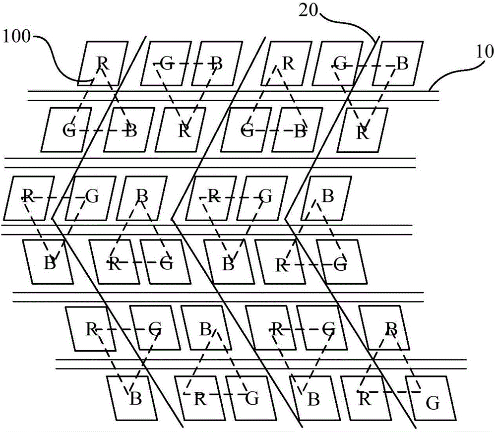
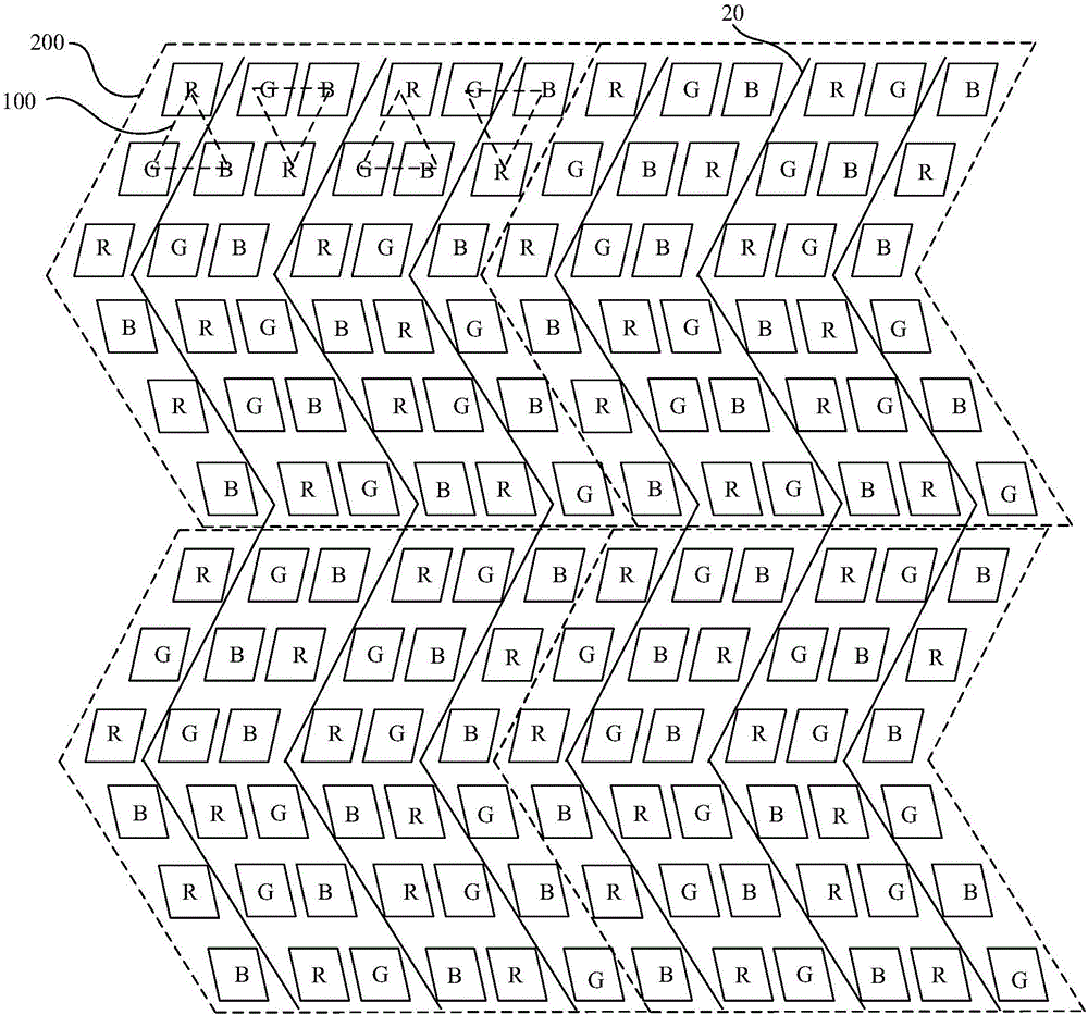
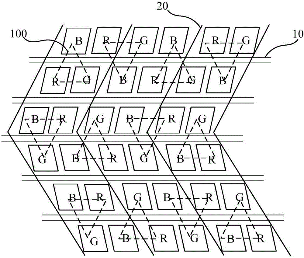
[0016] The present invention provides a display substrate, specifically a display substrate with a double-gate structure, which is used to solve the problem that the double-gate structure saves half of the data lines, resulting in differences in brightness between pixel regions and affecting display quality.

[0017] In order to solve the above technical problems, the present invention sets the display substrate to include a plurality of pixel repeating units, the number of pixel regions in all pixel repeating units is the same, and the sub-pixel regions are arranged in the same way, and each pixel region is composed of two adjacent The row consists of three adjacent sub-pixel regions. Each pixel repeating unit includes 2n rows*3m columns of sub-pixel areas. Since the pixel repeating unit includes an integer number of columns of sub-pixel areas, it overcomes the impact of saving half of the data lines on the brightness of the pixel repeating unit, ensuring that the brightness d...


PUM


Abstract

The invention relates to the technical field of display and discloses a display substrate and a display device. A display area for arranging the display substrate is composed of a plurality of same pixel repeating units and each pixel repeating unit comprises integer rows of pixel sub-regions, so that the problem of the display quality influenced by the luminance difference between the pixel regions resulted from the removal of a half of data lines from a double-grating structure can be solved, the consistent luminance distribution of all the pixel repeating units can be guaranteed, the luminance difference between the pixel repeating units can be reduced and the display quality can be promoted. The contradiction between the aperture opening ratio of the double-grating structure and the luminance distribution difference of the pixels can be solved without sacrificing the aperture opening ratio.

Description

technical field [0001] The present invention relates to the field of display technology, in particular to a display substrate and a display device. Background technique [0002] In the field of flat panel display technology, Thin Film Transistor Liquid Crystal Display (TFT-LCD) has the advantages of small size, low power consumption, and relatively low manufacturing cost, and gradually occupies a dominant position in today's flat panel display market. The main structure of TFT-LCD is the array substrate and the color filter substrate of the box. The array substrate includes a plurality of gate lines and a plurality of data lines intersecting to define a plurality of sub-pixel regions, and each pixel region is composed of a plurality of adjacent sub-pixel regions. Each sub-pixel area includes a pixel electrode and a thin film transistor. The gate electrode of the thin film transistor is electrically connected to the gate line, the source electrode is electrically connected t...

Claims


Application Information

Patent Timeline
IPC IPC(8): G02F1/1362H01L27/12G09G3/36
Inventor 赵伟利廖峰柳在健
Owner BOE TECH GRP CO LTD
Features
  • Generate Ideas
  • Intellectual Property
  • Life Sciences
  • Materials
  • Tech Scout
  • Unparalleled Data Quality
  • Higher Quality Content
  • 60% Fewer Hallucinations
Learn More