Method for checking defects of substrate glass, field terminal and server

A glass defect and on-site terminal technology, which is applied in the direction of optical testing defects/defects, instruments, scientific instruments, etc., can solve the problems of restricting production efficiency, restricting equipment resource sharing, consuming large manpower and material costs, and saving use and maintenance costs , Improve the defect detection rate and save the detection time

Inactive Publication Date: 2017-05-10
TUNGHSU TECH GRP CO LTD +1
View PDF5 Cites 7 Cited by
  • Summary
  • Abstract
  • Description
  • Claims
  • Application Information

AI Technical Summary

Problems solved by technology

And the process of neural network training requires a lot of professional and technical personnel to operate, and this process cannot provide effective basis for the manufacturer's process countermeasures, which restricts the improvement of production efficiency
[0005] Secondly, there is no theoretical guidance for the selection of the number of layers and the number of units in the hidden layer of the neural network. It is generally determined based on experience or through repeated experiments. resource sharing
[0006] In addition, the training of the classification model is a relatively complicated operation for general equipment users, and the training and maintenance of software operation also need to consume a lot of manpower and material resources.
In addition, the training process of the classification model depends on the subjectivity of the operator. The more operators there are, the greater the error will be.

Method used


Image

  • Method for checking defects of substrate glass, field terminal and server
  • Method for checking defects of substrate glass, field terminal and server
  • Method for checking defects of substrate glass, field terminal and server

Examples


Embodiment Construction

[0037] Specific embodiments of the present invention will be described in detail below in conjunction with the accompanying drawings. It should be understood that the specific embodiments described here are only used to illustrate and explain the present invention, and are not intended to limit the present invention.

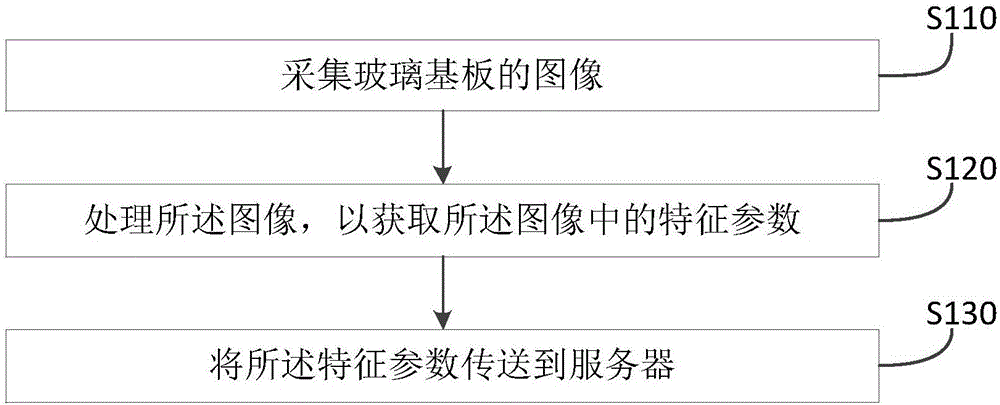
[0038] figure 1 is a flowchart of a method for inspecting substrate glass defects according to Embodiment 1 of the present invention. Such as figure 1 As shown, the method includes the following steps:

[0039] In step S110, an image of the substrate glass is collected. Wherein, the image of the substrate glass can be acquired by an image acquisition device, such as a line array CCD camera or an area array CCD camera, which can be installed in the production line of the substrate glass. When the substrate glass passes by, the line array CCD camera or the area array CCD camera The camera can capture in real time to obtain images of the substrate glass. In th...


PUM


Abstract

The invention relates to the field of manufacturing of displays and discloses a method for checking the defects of substrate glass. The method comprises the following steps: acquiring an image of the substrate glass; processing the image to acquire characteristic parameters in the image; transmitting the characteristic parameters to a server. On the other hand, the invention also provides a method for checking the defects of the substrate glass. The method comprises the following steps: receiving the characteristic parameters of the substrate glass image; classifying the characteristic parameters to obtain classifying results; transmitting the classifying results to a field terminal. The invention also provides the field terminal and the server applying the method, as well as a system applying the field terminal and the server. By using the technical scheme provided by the invention, the classifying work of the defects can be concentrated in the server for executing, so that the classifying efficiency and accuracy can be improved.

Description

technical field [0001] The invention relates to the field of display manufacturing, in particular to a method for inspecting substrate glass defects, a field terminal and a server. Background technique [0002] Ultra-thin display substrate glass is a key upstream material for manufacturing TFT-LCD (thin film transistor-liquid crystal display, thin film transistor liquid crystal display), OLED (organic light-emitting diode) and other displays. The quality of the substrate glass will affect the quality of the display, so customers have strict requirements on its defects, and identifying the defects of the substrate glass has become a necessary means of product quality control. At the same time, the identification of defect types (bubbles, stones, platinum particles, etc.) is also an important basis for adjusting and optimizing the production process. Therefore, in order to improve the defect detection rate before ensuring productivity, computer vision technology and neural ne...

Claims


Application Information

Patent Timeline
Patent Type & Authority Applications(China)
IPC IPC(8): G01N21/88G01N21/95
CPCG01N21/8851G01N21/95G01N2021/8887G01N2021/9513
Inventor 周波李青王丽红郑权
Owner TUNGHSU TECH GRP CO LTD
Why Eureka
Try Eureka