Packaging structure of implanted chip and manufacturing method thereof

A packaging structure and implantable technology, which is applied in semiconductor/solid-state device manufacturing, electrical components, electrical solid-state devices, etc., can solve the problems of circuit interface air tightness and biocompatibility, and the limited number of implanted electrodes. Achieve the effect of easy manipulation, simple method and easy industrialization

Active Publication Date: 2017-05-10
SHENZHEN INST OF ADVANCED TECH CHINESE ACAD OF SCI
View PDF8 Cites 5 Cited by
  • Summary
  • Abstract
  • Description
  • Claims
  • Application Information

AI Technical Summary

Problems solved by technology

[0004] The object of the present invention is to provide an implantable chip packaging structure, which aims to solve the above-mentioned series of problems existing in the existing implantable chip packaging structure, such as the airtightness and biocompatibility of the circuit interface, implanted electrode limited number of questions

Method used


Image

  • Packaging structure of implanted chip and manufacturing method thereof
  • Packaging structure of implanted chip and manufacturing method thereof
  • Packaging structure of implanted chip and manufacturing method thereof

Examples


Embodiment Construction

[0019] In order to make the technical problems, technical solutions and beneficial effects to be solved by the present invention clearer, the present invention will be further described in detail below in conjunction with the accompanying drawings and embodiments. It should be understood that the specific embodiments described here are only used to explain the present invention, not to limit the present invention.

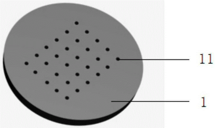
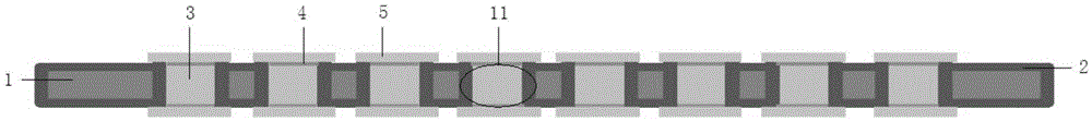
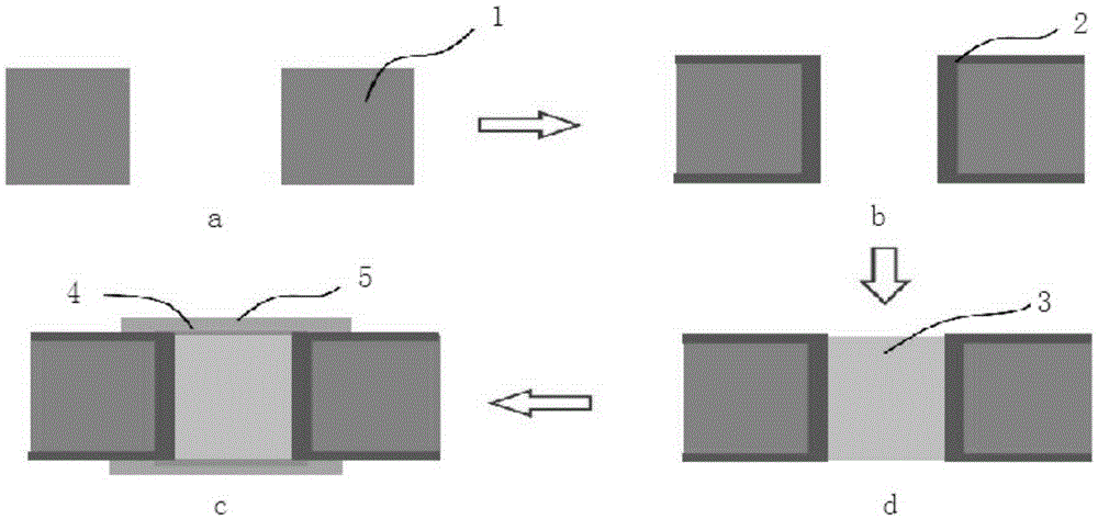
[0020] combine Figure 1-2 , the embodiment of the present invention provides an implantable chip packaging structure, including a base 1 and a plurality of through holes 11 penetrating through the base 1, the surface of the base 1 and the walls of the through holes 11 are provided with diamond layers 2. The through hole 11 covered by the diamond layer 2 is provided with an electrode lead 3, and the upper and lower surfaces of the electrode lead 3 are respectively provided with a transition metal layer 4 and a protective layer 5 in sequence, and the adjacent electr...


PUM


Abstract

The invention provides a packaging structure of an implanted chip and a manufacturing method thereof. The packaging structure of the implanted chip comprises a substrate and a plurality of through holes passing through the substrate. A substrate surface and through hole wall surfaces are provided with diamond layers. Electrode lead wires are arranged in the through holes wrapped by the diamond layers. Upper and low surfaces of the electrode lead wires are successively provided with a transition metal layer and a protection layer. The transition metal layer and the protection layer on the adjacent electrode lead wires are not connected. The protection layer is a doped diamond layer.

Description

technical field [0001] The invention belongs to the technical field of implanted chips, and in particular relates to a packaging structure of implanted chips and a preparation method thereof. Background technique [0002] An implantable chip is a tiny chip that can be implanted in an animal to function, such as an implanted artificial retina chip. Existing implantable chips such as artificial retinal chips are not biologically compatible, and the chip interacts with the microenvironment in the human body, which will lead to corrosion of the chip after a long time and pose a safety hazard to the human body. Therefore, it is particularly important to package the chip in a biocompatible and highly airtight package. Biocompatible packaging requires that the cavity has good airtightness, certain mechanical support performance and tensile strength performance, and the use of packaging materials meets the requirements of biocompatibility, appearance flatness and internal smoothnes...

Claims


Application Information

Patent Timeline
Patent Type & Authority Applications(China)
IPC IPC(8): H01L23/31H01L23/29H01L21/56
CPCH01L23/31H01L21/561H01L23/291H01L23/3157
Inventor 杨扬唐永炳李刚
Owner SHENZHEN INST OF ADVANCED TECH CHINESE ACAD OF SCI
Why Eureka
Try Eureka