

Shifting register, GOA circuit, driving method thereof and display device
A technology of shift register and potential, applied in the fields of GOA circuit and its driving method, shift register, and display device, to achieve the effects of saving layout space, stable output, and increasing anti-noise ability
- Summary
- Abstract
- Description
- Claims
- Application Information
AI Technical Summary
Problems solved by technology
Method used
Image

Examples
Embodiment 1
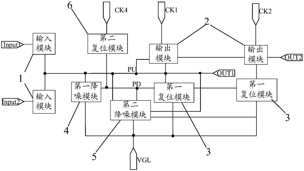
[0044] This embodiment provides a shift register, such as figure 1 As shown, it includes: a plurality of input modules 1, a plurality of output modules 2, a first reset module 3 corresponding to each input module 1, a first noise reduction module 4, a second noise reduction module 5, and a second reset module 6.
[0045] Wherein, in this embodiment, two input modules 1 and two output modules 2 are used for illustration, and the case of three or more input modules 1 and output modules 2 is similar to this embodiment.
[0046] Each input module 1 is connected to the pull-up node PU and its corresponding signal input terminals Input1 and Input2, and is used to charge the pull-up node PU under the control of the signal input by the signal input terminal;
[0047]Each output module 2 is connected to the pull-up node PU, the signal output terminals OUT1 and OUT2 corresponding to each, the first clock control signal terminals CK1 and CK2 corresponding to each, and the first reset mo...
Embodiment 2
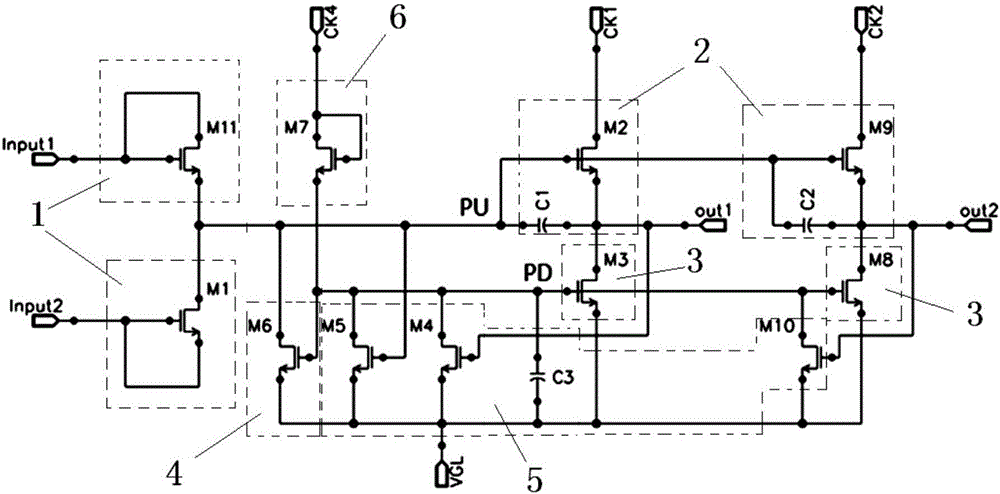
[0055] This embodiment provides a shift register, such as figure 2 As shown, it includes: two input modules 1, two output modules 2, a first reset module 3 corresponding to each input module 1, a first noise reduction module 4, a second noise reduction module 5, and a second reset module 6.
[0056] in, figure 2 The upper left is the first input module 1, the lower left is the second input module 1, the upper middle is the first output module 2, and the upper right is the second output module 2.
[0057] The shift register of this embodiment has four clock control signal terminals CK1, CK2, CK3, and CK4, wherein CK1, CK2, CK3, and CK4 are clock signals with a difference of 1 / 4 cycle in sequence.
[0058] Each input module 1 includes a first transistor, the control electrode and the first stage of the first transistor are connected to the signal input terminal Input1 corresponding to the input module 1 , and the second stage of the first transistor is connected to the pull-...
Embodiment 3
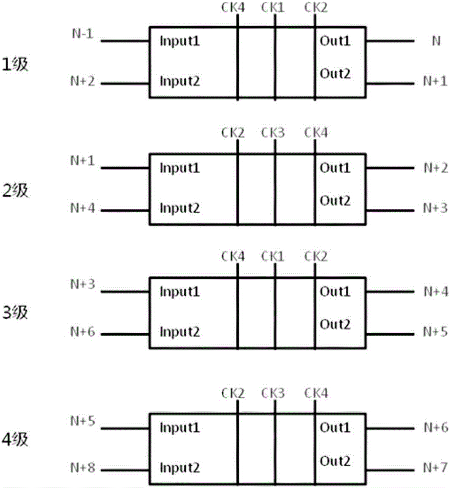
[0077] This embodiment provides a GOA circuit, including a plurality of cascaded shift registers of the foregoing embodiments.
[0078] GOA cascade see image 3 , Odd-numbered shift registers, such as 1-stage shift registers are controlled by CK1, CK2, CK4 clock control signal terminals; even-numbered stage shift registers, such as 2-stage shift registers are controlled by CK3, CK4, CK2 clock control signal terminals ;So on and so forth. figure 2 Among them, Input1 is the output signal N-1 of the upper stage, and Input2 is the signal N+2 output by the lower stage. Out1 is the first output signal N of the current stage, and Out2 is the second output signal N+1 of the current stage.
[0079] This embodiment also provides a driving method for the above-mentioned GOA circuit, see Figure 4 , the method includes:
[0080] In the first stage t1, the first input module 1 charges the pull-up node PU under the control of the signal input from the first signal input terminal Input1...
PUM
 Abstract
Description
Claims
Application Information