Fingerprint recognition chip packaging structure and method

A technology of chip packaging structure and fingerprint recognition, which is applied in character and pattern recognition, acquisition/organization of fingerprints/palmprints, instruments, etc. It can solve the problems of electrical signal crosstalk and reduce the accuracy of fingerprint recognition, so as to avoid crosstalk and reduce the production cost. Effect of cost, high mechanical strength

Inactive Publication Date: 2017-05-17
CHINA WAFER LEVEL CSP
View PDF0 Cites 10 Cited by
  • Summary
  • Abstract
  • Description
  • Claims
  • Application Information

AI Technical Summary

Problems solved by technology

Preparing so many pixels for a fingerprint recognition that is only pressed by one finger can easily cause...

Method used


Image

  • Fingerprint recognition chip packaging structure and method
  • Fingerprint recognition chip packaging structure and method
  • Fingerprint recognition chip packaging structure and method

Examples


Embodiment Construction

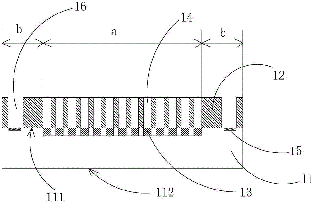
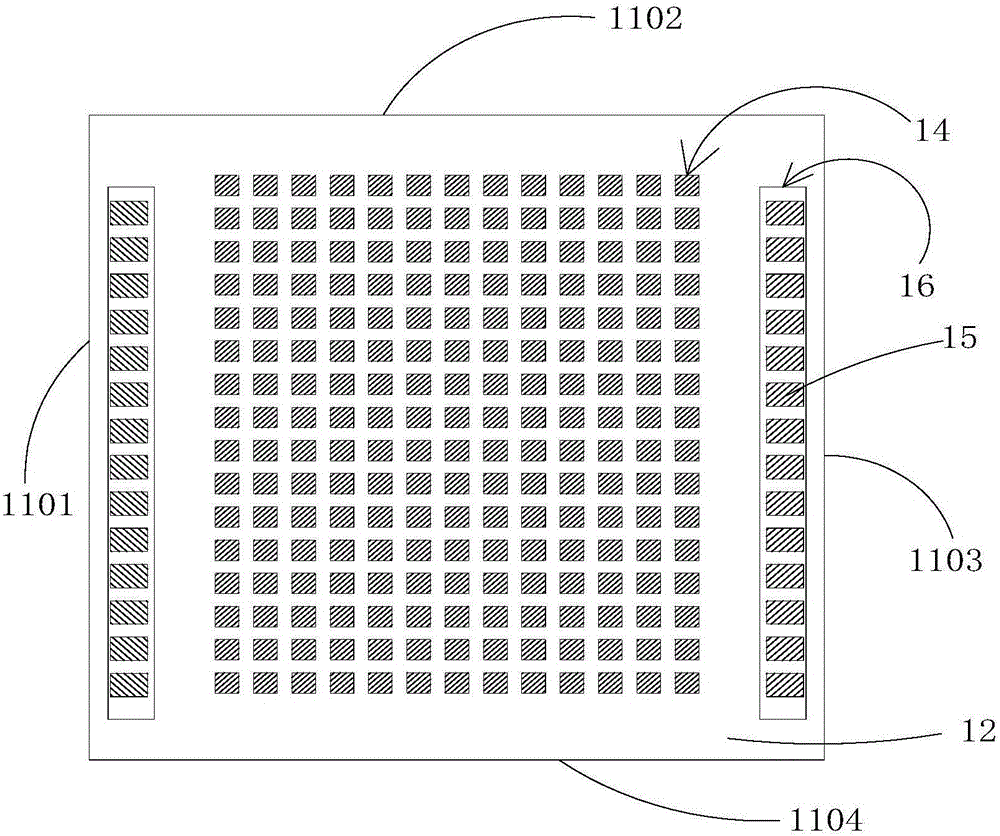
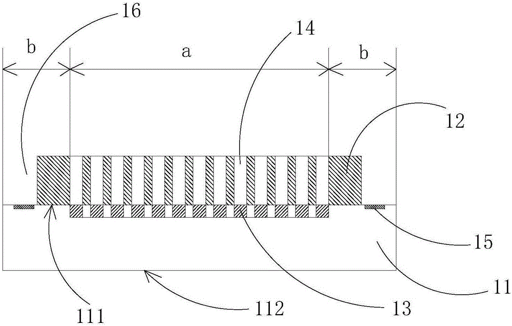
[0045] Specific embodiments of the present invention will be described in detail below in conjunction with the accompanying drawings. However, these embodiments do not limit the present invention, and any structural, method, or functional changes made by those skilled in the art according to these embodiments are included in the protection scope of the present invention.

[0046] It should be noted that the purpose of providing these drawings is to facilitate the understanding of the embodiments of the present invention, and should not be interpreted as undue limitations on the present invention. For clarity, the dimensions shown in the figures are not drawn to scale and may be enlarged, reduced or otherwise changed. In addition, the three-dimensional space dimensions of length, width and depth should be included in actual production. Additionally, configurations described below in which a first feature is "on" a second feature may include embodiments where the first and seco...


PUM

PropertyMeasurementUnit
Thicknessaaaaaaaaaa

Abstract

The invention provides a fingerprint recognition chip packaging structure and method. The structure comprises a fingerprint recognition chip and a silicone cover plate. The fingerprint recognition chip comprises a front face and a rear face opposite to the front face. The front face of the fingerprint recognition chip is provided with a fingerprint recognition region and multiple welding pads located on the periphery of the fingerprint recognition region. The welding pads are electrically coupled with the fingerprint recognition region. The fingerprint recognition region is composed of multiple pixel points arranged in an array mode, and the pixel points are used for acquiring fingerprint information. The silicone cover plate is pressed on the front face of the fingerprint recognition chip, multiple through holes are formed in the portion, corresponding to the fingerprint recognition region, of the silicone cover plate, the through holes correspond to the pixel points one to one, and the pixel points are exposed at the bottoms of the through holes. The welding pads are exposed on the silicone cover plate. The silicone cover plate has the low dielectric constant, the crosstalk problem between the adjacent pixel points can be reduced, and the accuracy of fingerprint recognition is improved.

Description

technical field [0001] The invention relates to the technical field of semiconductor chip packaging, in particular to a packaging structure and a packaging method of a fingerprint identification chip. Background technique [0002] With the continuous advancement of science and technology, more and more electronic devices are widely used in people's daily life and work, which brings great convenience to people's daily life and work, and has become an indispensable tool for people today. . With the increasing functions of electronic devices, more and more important information is stored in electronic devices, and the identity verification technology of electronic devices has become a main direction of research and development of electronic devices. [0003] Due to the uniqueness and invariance of fingerprints, fingerprint identification technology has many advantages such as good security, high reliability and simple use. Therefore, fingerprint identification technology has ...

Claims


Application Information

Patent Timeline
IPC IPC(8): H01L23/31H01L21/50H01L21/56G06K9/00
CPCH01L24/94H01L21/50H01L21/561H01L23/3107G06V40/13G06V40/1306H01L2224/48091H01L2224/73265H01L2924/00014
Inventor 王之奇
Owner CHINA WAFER LEVEL CSP
Why Eureka
Try Eureka