Semiconductor structure and fabricating method thereof

A technology of semiconductor and epitaxial structure, applied in semiconductor/solid-state device manufacturing, semiconductor device, semiconductor/solid-state device testing/measurement, etc., can solve problems such as increasing the complexity of semiconductor devices

Inactive Publication Date: 2017-05-17
TAIWAN SEMICON MFG CO LTD
View PDF0 Cites 6 Cited by
  • Summary
  • Abstract
  • Description
  • Claims
  • Application Information

AI Technical Summary

Problems solved by technology

However, the increased density of IC devices such as transistors has also incre

Method used


Image

  • Semiconductor structure and fabricating method thereof
  • Semiconductor structure and fabricating method thereof
  • Semiconductor structure and fabricating method thereof

Examples


Embodiment Construction

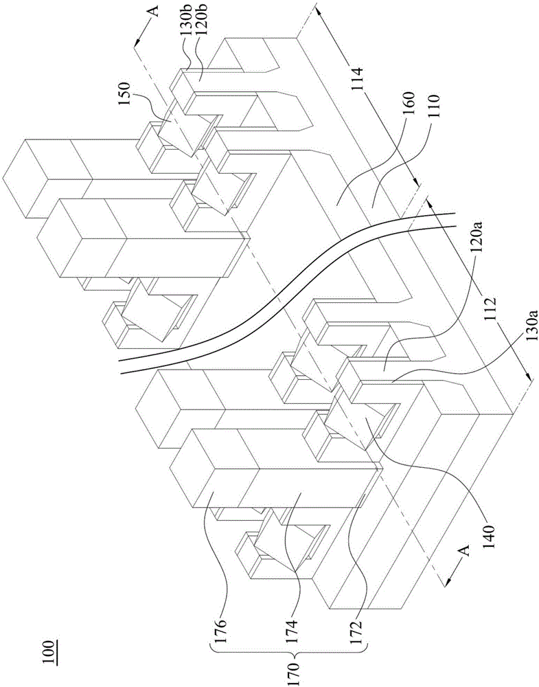
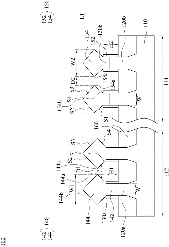
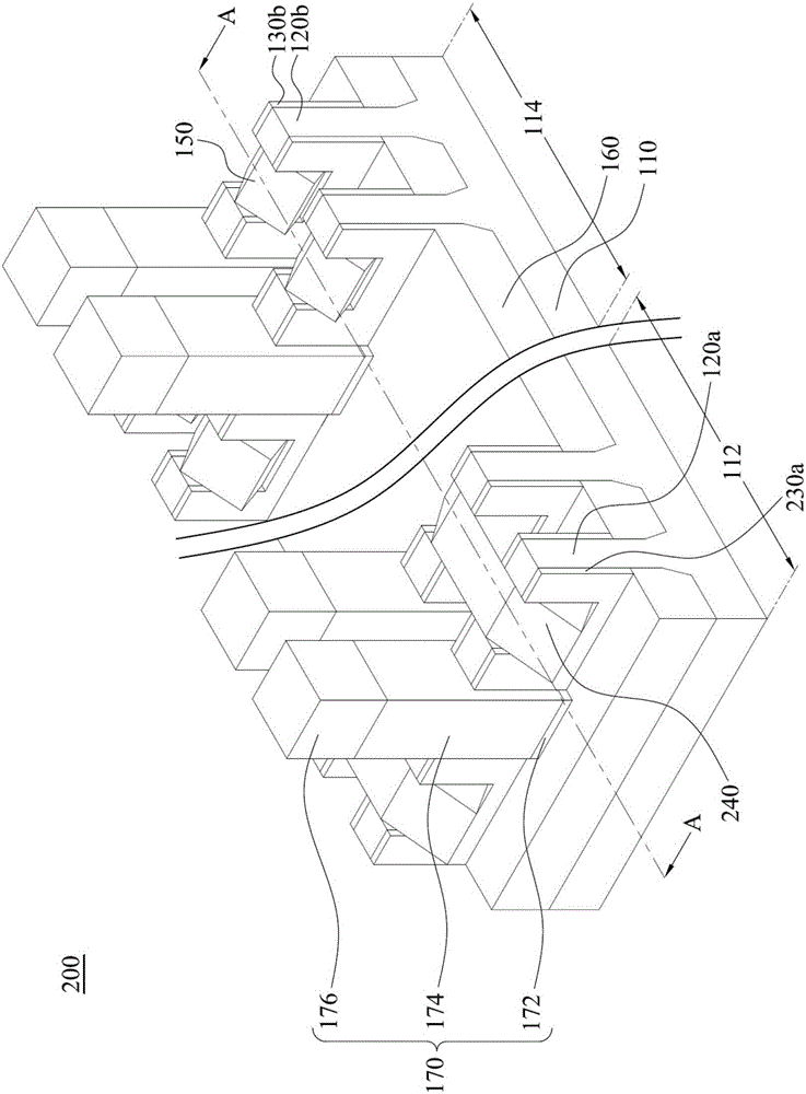
[0014] The following disclosure provides many different embodiments or examples for implementing different features of the presented subject matter. Specific examples of components and arrangements are described below to simplify the present disclosure. Of course, these are examples only and are not intended to limit the invention. For example, in the following description, forming a first component on or on a second component may include an embodiment in which the first component and the second component are formed in direct contact, and may also include an embodiment in which an additional component may be formed between the first component and the second component. An instance of a component such that the first component and the second component may not be in direct contact. In addition, the present invention may repeat reference numerals and / or characters in various embodiments. This repetition is for the sake of simplicity and clarity and does not in itself indicate a r...


PUM


Abstract

A semiconductor structure includes a device region and a test region. In the device region, first fin spacers cover sidewalls of a first fin structure and have a first height, and a first epitaxy structure is disposed in the first fin structure, which a portion of the first epitaxy structure is above the first fin spacers and having a first width. In the test region, second fin spacers cover sidewalls of the second fin structure and have a second height, and the second height is greater than the first height. A second epitaxy structure is disposed in the second fin structure, and a portion of the second epitaxy structure is above the second fin spacers and having a second width, which the second width is less than the first width.

Description

technical field [0001] Embodiments of the present invention relate to integrated circuit devices, and more particularly, to semiconductor structures and methods of fabrication thereof. Background technique [0002] The manufacture of integrated circuits (ICs) has been greatly driven by the need to increase the density of integrated circuits formed in semiconductor devices. This is usually done by enforcing more aggressive design rules to allow greater density of formed IC devices. However, the increased density of IC devices such as transistors has also increased the complexity of handling semiconductor devices with reduced feature sizes. [0003] For example, semiconductor devices such as Fin Field Effect Transistors (FinFETs) have been scaled down through various technology nodes, using epitaxial (epi) semiconductor materials have achieved strained source / drain features (e.g., stressor regions) for enhanced current carrying ion mobility and improve device performance. F...

Claims


Application Information

Patent Timeline
IPC IPC(8): H01L29/78H01L21/336H01L29/06
CPCH01L22/30H01L21/823807H01L21/823814H01L21/823821H01L27/0924H01L29/045H01L29/0653H01L29/0847H01L29/161H01L29/165H01L29/7848H01L29/785H01L29/06H01L29/66795
Inventor 宋学昌张智强李昆穆
Owner TAIWAN SEMICON MFG CO LTD
Why Eureka
Try Eureka