Display device and method of manufacturing same
A technology for a display device and a display area, which is applied in semiconductor/solid-state device manufacturing, instruments, organic semiconductor devices, etc., and can solve problems such as scratches on blocking components, defects in the film encapsulation structure, and cracks
- Summary
- Abstract
- Description
- Claims
- Application Information
AI Technical Summary
Problems solved by technology
Method used
Image
Examples
Embodiment Construction
[0103] Hereinafter, embodiments will be explained in detail with reference to the accompanying drawings. In this disclosure, the term "substantially" includes completely, nearly completely, or in some applications and according to those skilled in the art, any significant degree. Furthermore, "formed, disposed or located on" can also mean "formed, disposed or located on". The term "connected" includes electrical connections.
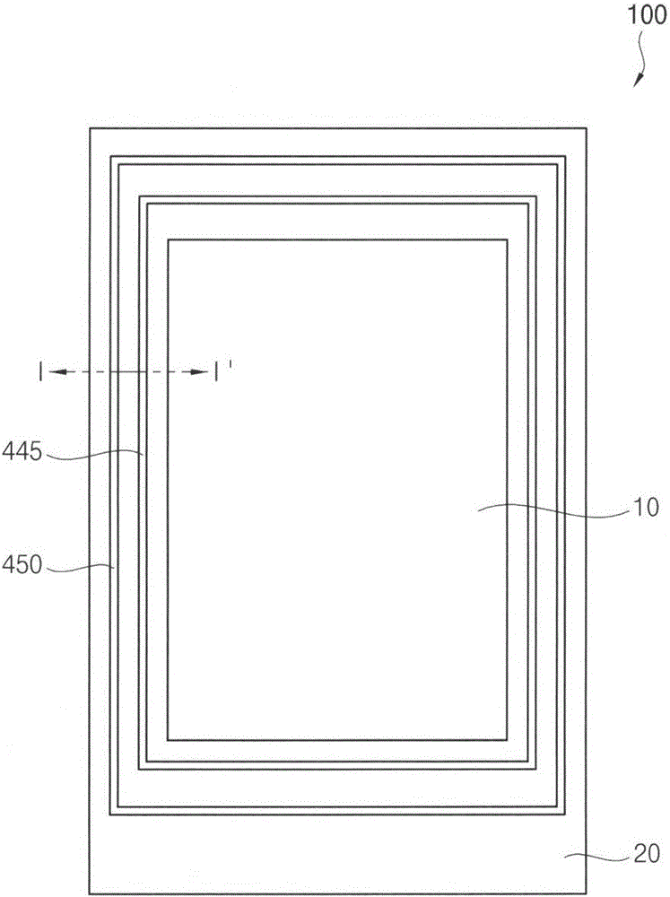
[0104] figure 1 is a plan view illustrating a display device according to example embodiments.
[0105] refer to figure 1 , the display device 100 includes a display area 10 and a peripheral area 20 .
[0106] A display structure can be provided in the display area 10 . The display image can be displayed in the display area 10 through a display structure (for example, organic light emitting diode, liquid crystal, etc.). Wires (eg, scan lines, data lines, power supply voltage lines, etc.) may be disposed in the peripheral area 20 . Here, wires may ...
PUM
 Abstract
Description
Claims
Application Information


