Display panel manufacturing method, display panel and display device

A display panel and manufacturing method technology, applied in semiconductor/solid-state device manufacturing, semiconductor devices, electrical components, etc., can solve the inconsistency of evaporation results of thin-film packaging layers, reduce the packaging effect of thin-film packaging layers, and easily deform the mask, etc. question

Active Publication Date: 2017-05-24
SHANGHAI TIANMA MICRO ELECTRONICS CO LTD
View PDF4 Cites 27 Cited by
  • Summary
  • Abstract
  • Description
  • Claims
  • Application Information

AI Technical Summary

Problems solved by technology

These particles will reduce the encapsulation effect of the thin film encapsulation layer
In addition, when aligning the mask with the display panel on which the thin-film encapsulation layer is to be fabricated, due to factors such as the limitation of equipment accura

Method used


Image

  • Display panel manufacturing method, display panel and display device
  • Display panel manufacturing method, display panel and display device
  • Display panel manufacturing method, display panel and display device

Examples


Embodiment Construction

[0033] The present invention will be further described in detail below in conjunction with the accompanying drawings and embodiments. It should be understood that the specific embodiments described here are only used to explain the present invention, but not to limit the present invention. In addition, it should be noted that, for the convenience of description, only some structures related to the present invention are shown in the drawings but not all structures.

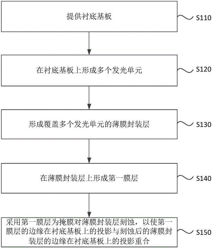
[0034] figure 1 It is a flow chart of a method for manufacturing a display panel provided by an embodiment of the present invention. see figure 1 , the manufacturing method of the display panel includes:

[0035] S110, providing a base substrate.

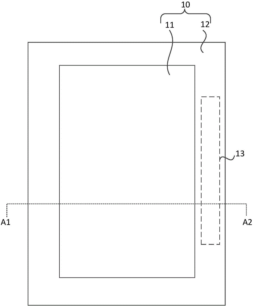
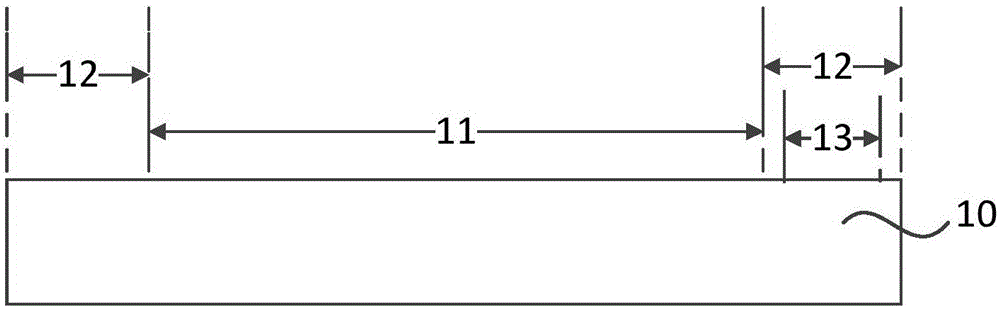
[0036] Figure 2a A schematic structural diagram of a base substrate provided in this embodiment. Figure 2b for along Figure 2a Schematic diagram of the cross-sectional structure of A1-A2. see Figure 2a and Figure 2b , providing a base substrate 10 . The b...


PUM


Abstract

The embodiment of the invention discloses a display panel manufacturing method, a display panel and a display device. The display panel manufacturing method comprises the steps of providing a substrate base plate; forming multiple light emitting units on the substrate base plate; forming a thin film packaging layer that covers the multiple light emitting units; forming a first film layer on the thin film packaging layer, wherein the distance between a projection, positioned on the substrate base plate, of a margin of a driver chip binding area on the display panel, which is adjacent to the light emitting units, and a projection, positioned on the substrate base plate, of a margin of the first film layer, which is adjacent to the driver chip binding area, is greater than or equal to 0 micron, or less than or equal to 100 microns; and positioning the projection, positioned on the substrate base plate, of the first film layer within a projection, positioned on the substrate base plate, of the thin film packaging layer; and to etching the thin film packaging layer by adopting the first film layer as a covering film so as to overlap the projection, positioned on the substrate base plate, of the margin of the first film layer generate and the projection, positioned on the substrate base plate, of the margin of the thin film packaging layer subjected to etching. According to the display panel manufacturing method, the display panel and the display device disclosed by the embodiment of the invention, the packaging effect of the thin film packaging layer in an organic light emitting display panel can be improved.

Description

technical field [0001] Embodiments of the present invention relate to a display panel manufacturing technology, and in particular, to a display panel manufacturing method, a display panel, and a display device. Background technique [0002] Organic light emitting display (Organic light emitting display), due to its technical advantages such as no need for backlight, high contrast, thin thickness, wide viewing angle, and fast response speed, has become one of the key directions for the development of the display industry. [0003] Since the organic light-emitting display panel is easily corroded by moisture and oxygen in the air, the display effect of the display panel deteriorates. At present, a thin film encapsulation layer is mainly used to prevent water vapor or oxygen in the air from entering into the organic light emitting display panel. When making an organic light-emitting display panel, a thin-film encapsulation layer is formed by vacuum coating. Specifically, the ...

Claims


Application Information

Patent Timeline
IPC IPC(8): H01L27/32H01L51/52H01L51/56
CPCH10K59/10H10K50/844H10K71/00
Inventor 蔡雨李喜烈刘聪慧于泉鹏
Owner SHANGHAI TIANMA MICRO ELECTRONICS CO LTD
Why Eureka
Try Eureka