Inclined slit based automatic focusing method and device

A technology of slits and tilt angles, which is applied in the field of semiconductor measurement, can solve problems such as difficulty in ensuring accuracy and difficulty in establishment, and achieves the effect of simple devices and structures and low cost

Active Publication Date: 2017-05-31
RAINTREE SCI INSTR SHANGHAI
View PDF12 Cites 18 Cited by
  • Summary
  • Abstract
  • Description
  • Claims
  • Application Information

AI Technical Summary

Problems solved by technology

In fact, due to the tilt of the wafer, especially the deformation of the wafer surface caused by vacuum adsorption, the premise of this method is difficult to hold in practice.
In addition, the non-uniformity of slit illumination and the difference in the reflectivity of each layer pattern, especially the unavoidable speckle noise of laser illumination, will affect the position detection of the peak pixel point of the slit confocal image, so the accuracy of the result sex is difficult to guarantee

Method used


Image

  • Inclined slit based automatic focusing method and device
  • Inclined slit based automatic focusing method and device
  • Inclined slit based automatic focusing method and device

Examples


Embodiment Construction

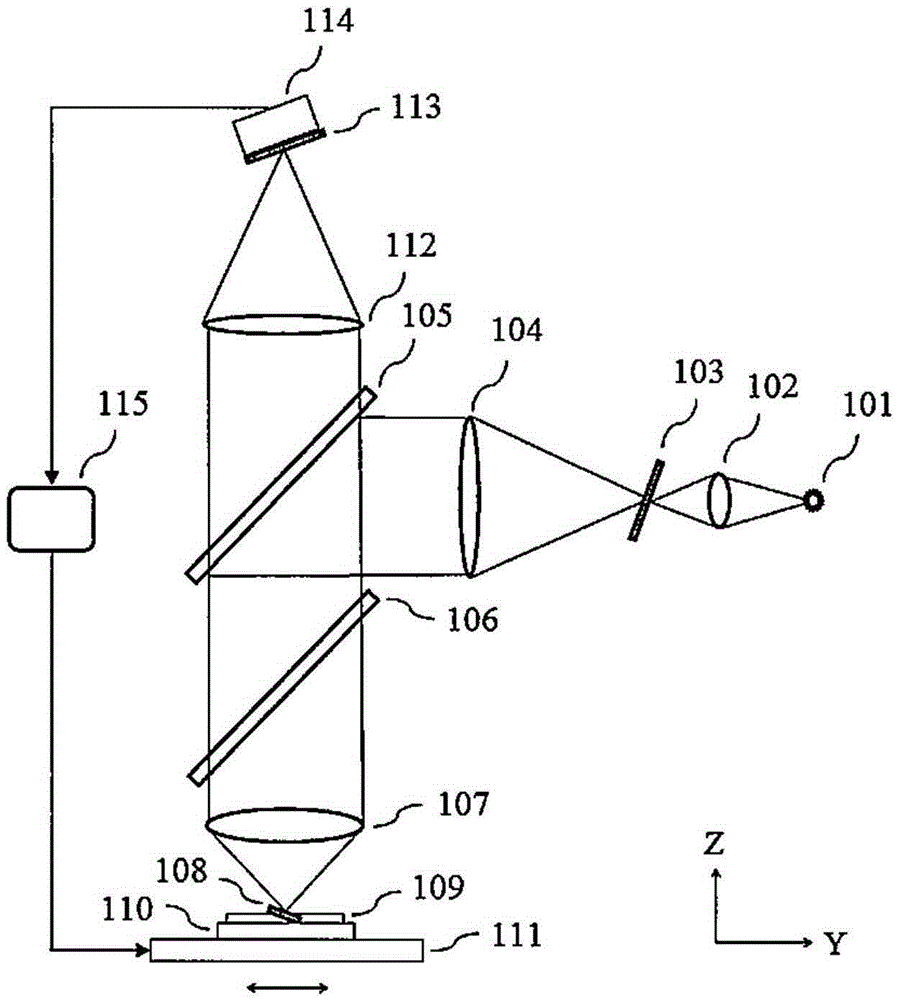
[0020] The patent of the present invention proposes a new defocus detection and autofocus method and corresponding system. The autofocus method proposed in the patent of the present invention is not only not affected by fluctuations in light intensity of the light source, nor affected by differences in wafer pattern shape and reflectivity, but also simpler in optical structure than patent US4639587 and patent US7961763B2.

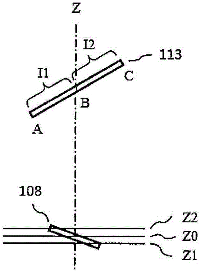
[0021] figure 1 An embodiment of the autofocus system of the present invention based on the oblique slit confocal method is shown. The hardware configuration of this embodiment is as follows: the illumination part is composed of a light source 101 and an illumination lens 102, and the light source 101 is an incoherent light source (such as LED). The oblique slit confocal imaging optical system consists of an illumination slit 103 , a lens 104 , a beam splitter 105 , an objective lens 107 , a lens 112 and a detection slit 113 . The arrangement of the lens ...


PUM


Abstract

The invention discloses an inclined slit based automatic focusing method and device. The device comprises an illumination unit, a beam splitting unit, an object lens (107) and a detection unit; the illumination unit comprises a light source (101), an illumination lens (102) and an illumination slit (103), and is used to provide incident light; the beam splitting unit carries out beam splitting on received light; the object lens (107) carries out imaging on the illumination slit (103) in the surface of a to-be-measured object (109), and reflects an image of the illumination slit (103) to the beam splitting unit; and the detection unit comprises a detection slit (113) and a detector (114), receives the image of the illumination slit (103) from the beam splitting unit and records a confocal signal related to the surface of the to-be-measured object (109), and the detection slit (113) and the illumination slit (103) are arranged inclinedly in the same inclination angles relative to the optical axes of themselves, and is positioned in a confocal position relative to the objective lens (7).

Description

technical field [0001] The invention belongs to the field of semiconductor measurement, and in particular relates to an automatic focusing method and system for wafer detection equipment with patterns on the surface. Background technique [0002] In the manufacturing process of integrated circuit chips, the product yield is an important indicator to measure the chip manufacturing process. As the critical dimensions of integrated circuits continue to shrink and the pattern density continues to increase, the difficulty of process control also increases. Defects that could be ignored in the past may cause the device to not work properly and become a fatal defect that affects the yield. At the same time, new three-dimensional device structures, such as FinFET, and new semiconductor materials (such as copper interconnects, low-k and high-k dielectric materials, and metal gate electrodes) are widely used, bringing new electrical performance defects; new process Processes, such as...

Claims


Application Information

Patent Timeline
Patent Type & Authority Applications(China)
IPC IPC(8): G02B7/28
CPCG02B7/28
Inventor 钟向红唐安伦徐益平
Owner RAINTREE SCI INSTR SHANGHAI
Why Eureka
Try Eureka