Digital wave-by-wave current limiting system and protection method based on fpga
A current limiting, wave-by-wave technology, applied in general control systems, control/regulation systems, program control, etc., can solve the problems of microprocessor interaction, information difficulty, and high overcurrent protection thresholds, and achieve improved safety, stability, Efficient fault tolerance mechanism and fast operation speed
- Summary
- Abstract
- Description
- Claims
- Application Information
AI Technical Summary
Problems solved by technology
Method used
Image
Examples
Embodiment 1
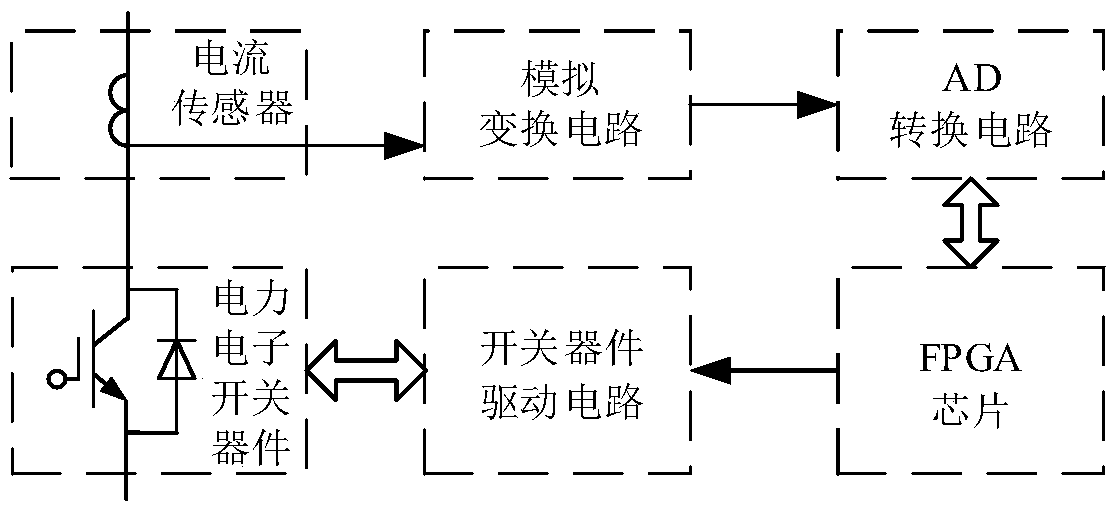
[0026] Such as figure 1 As shown, a FPGA-based digital wave-by-wave current limiting system includes a current measurement circuit, a power electronic switching device and a switching device drive circuit, and also includes an analog conversion circuit, an AD conversion circuit and an FPGA chip, wherein the current measurement circuit detects that the switch The current of the device is transformed by the analog conversion circuit into a signal suitable for the acquisition of the AD conversion circuit, which is converted into a digital signal by the AD conversion circuit. The FPGA chip acquires the digital signal, performs over-current judgment, and outputs the duty ratio of the pulse width signal to the switching device. The circuit drives power electronic switching devices.
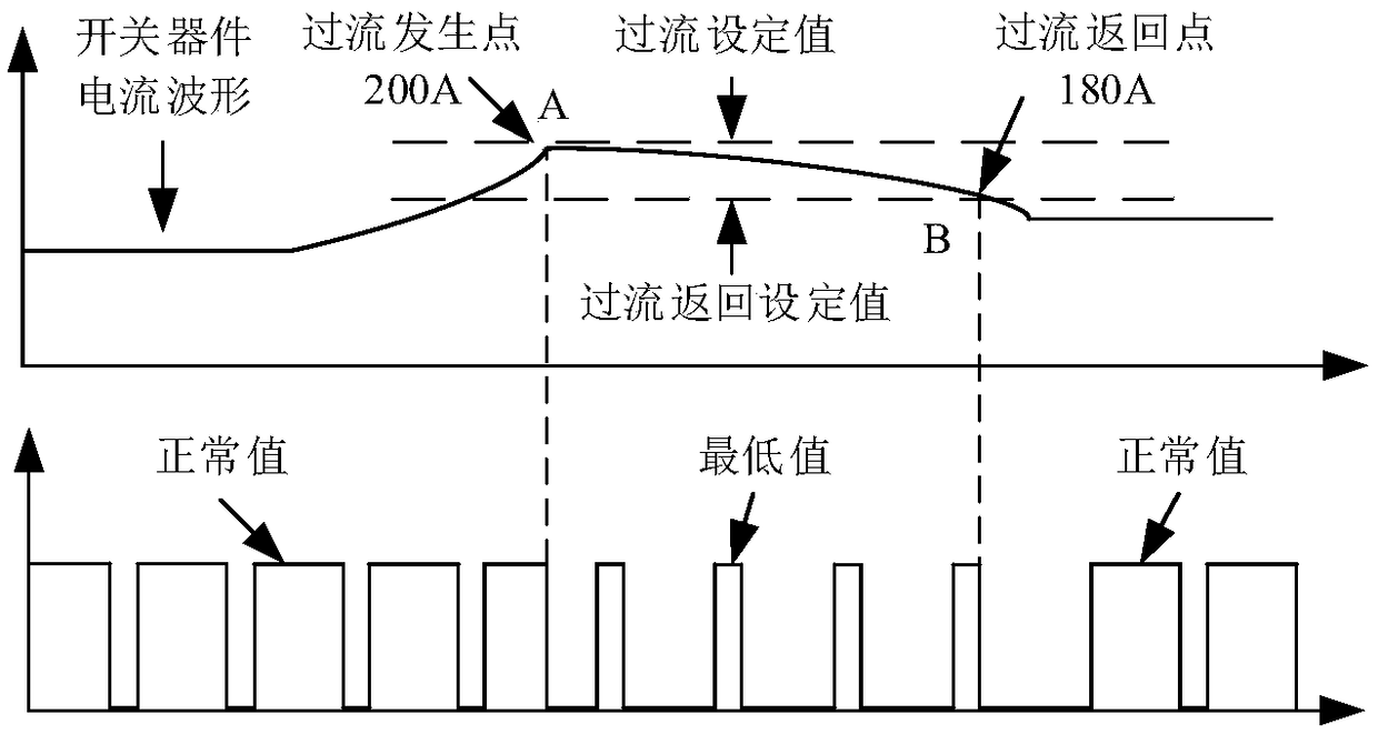
[0027] A kind of current protection method of the above-mentioned digitization wave-by-wave current limiting system based on FPGA, such as image 3 and Figure 4 shown, including the following steps: ...
Embodiment 2
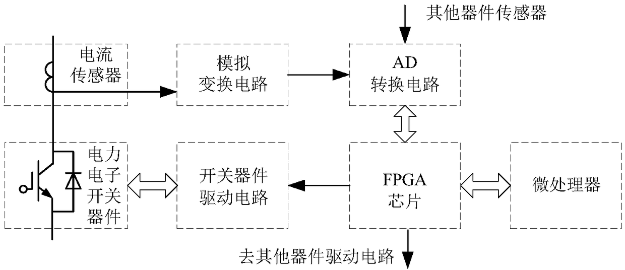
[0035] The basic principle of this embodiment is the same as that of Embodiment 1, the difference is that: figure 2 As shown, there are several power electronic switching devices, and each power electronic switching device corresponds to a group of current measurement circuits, switching device drive circuits, analog conversion circuits and AD conversion circuits, and each AD conversion circuit is respectively connected to the described The FPGA chip is connected, and the FPGA chip is respectively connected with each switching device driving circuit.
[0036] Several of the AD conversion circuits can be integrated into an AD chip, and the user can determine the number of channels, sampling bits and sampling rate of the AD chip according to the actual object requirements. When the AD chip is multi-channel, the current sampling of multiple switching devices can be completed at the same time, providing support for realizing the wave-by-wave current limitation of multiple devices...
PUM
 Abstract
Description
Claims
Application Information


