Semiconductor device

A semiconductor and device technology, applied in the field of semiconductor devices, can solve problems such as diode loss

Active Publication Date: 2019-07-02
DENSO CORP
View PDF5 Cites 0 Cited by
  • Summary
  • Abstract
  • Description
  • Claims
  • Application Information

AI Technical Summary

Problems solved by technology

Diode loss due to the flow of reverse recovery current (so-called reverse recovery loss)

Method used


Image

  • Semiconductor device
  • Semiconductor device
  • Semiconductor device

Examples


Embodiment Construction

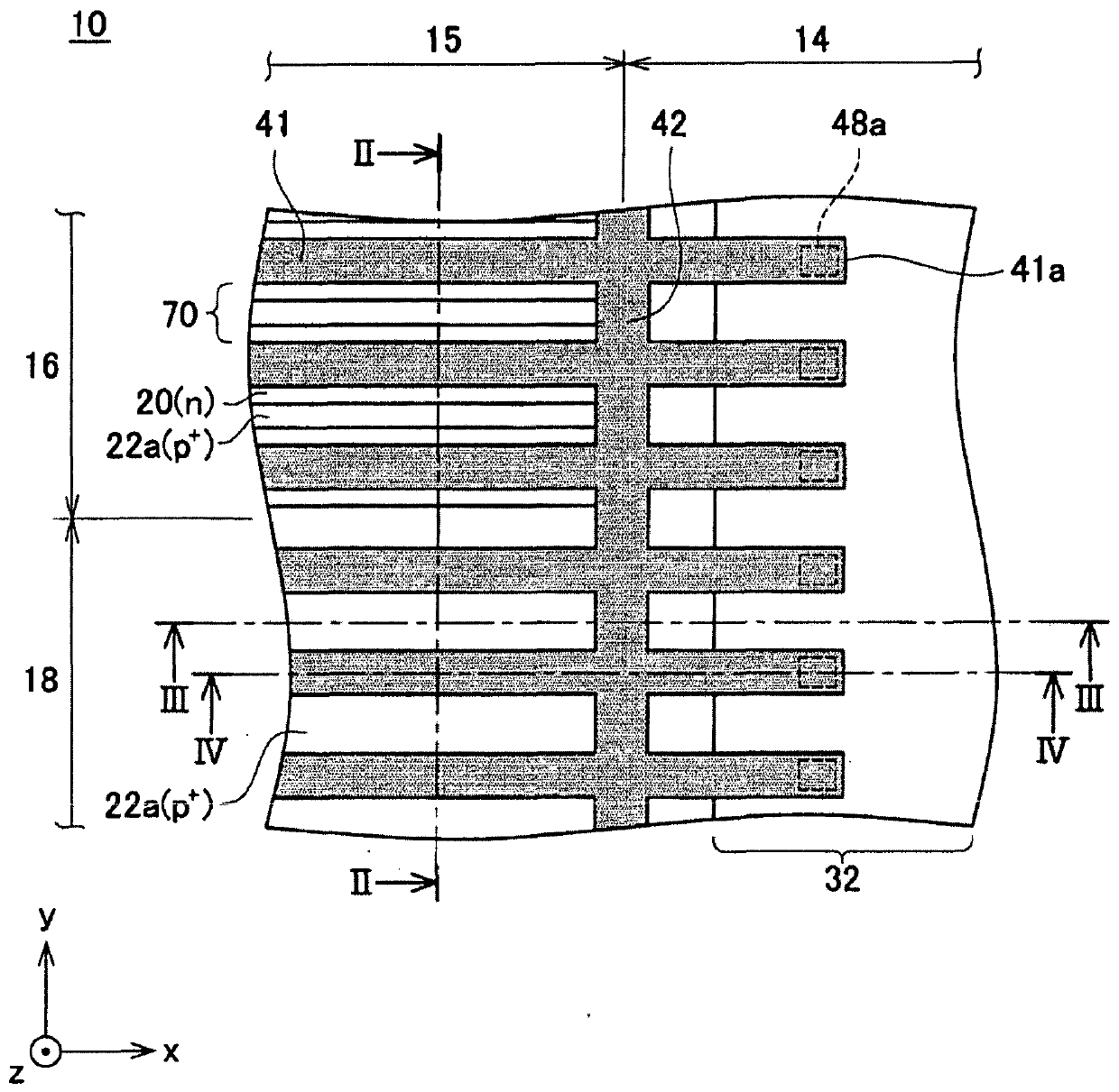
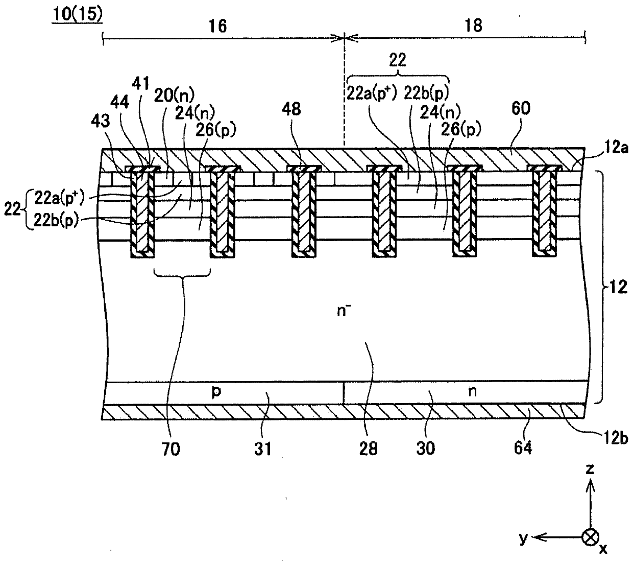
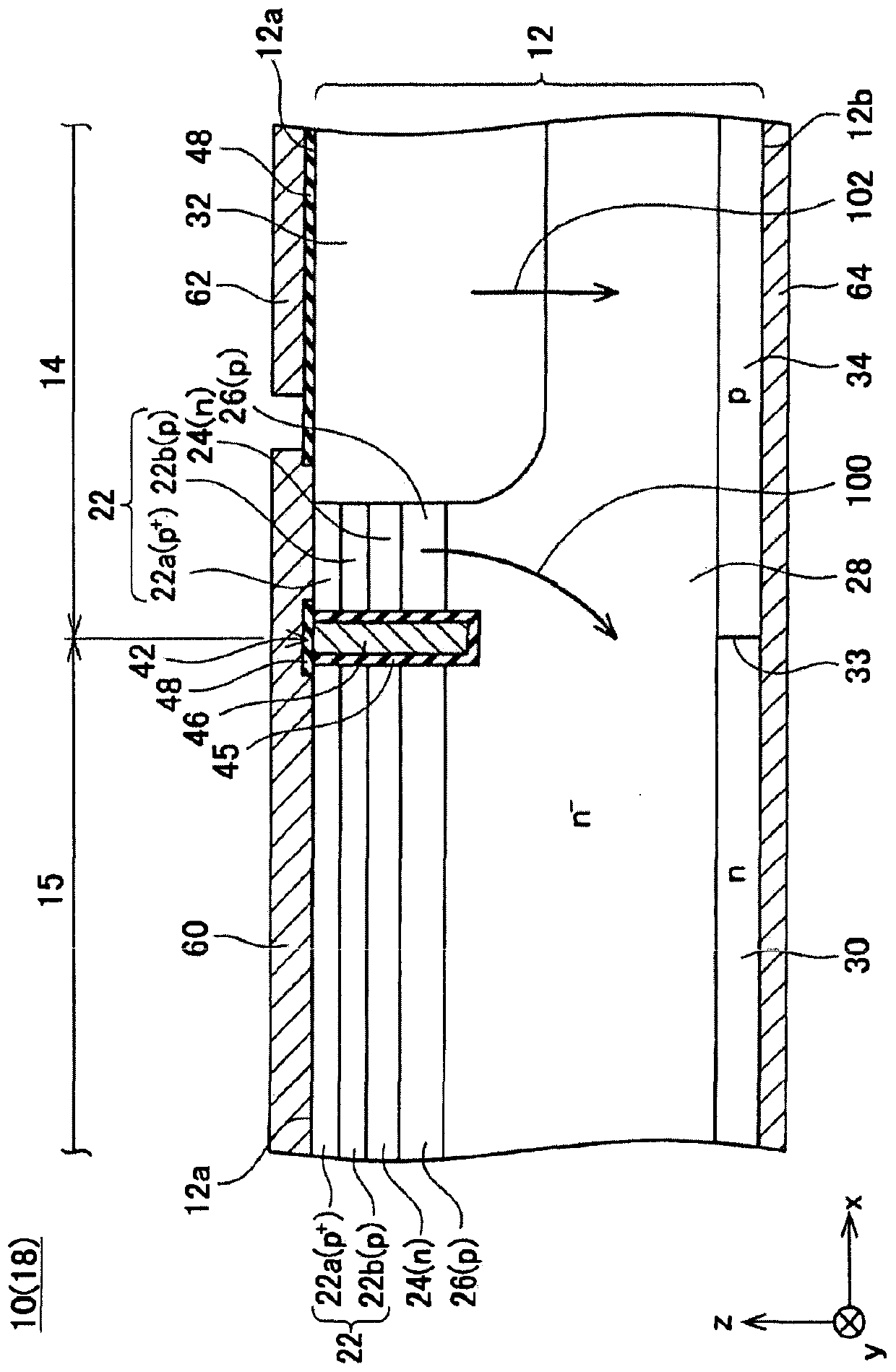
[0022] Figures 1 to 4 An example semiconductor device 10 is shown. The semiconductor device 10 has a semiconductor substrate 12 and electrodes, insulating films, and the like arranged on the upper surface 12 a and the lower surface 12 b of the semiconductor substrate 12 . Note that in order to facilitate understanding of the drawings, electrodes and insulating layers on the semiconductor substrate 12 are figure 1 is not shown. Also, to facilitate the visibility of the drawings, the figure 1 The first trench 41 and the second trench 42 are hatched. In the following description, the direction parallel to the upper surface 12a of the semiconductor substrate 12 is referred to as the x direction, the direction parallel to the upper surface 12a of the semiconductor substrate 12 and orthogonal to the x direction is referred to as the y direction, and the direction of the semiconductor substrate 12 The thickness direction is referred to as the z direction.

[0023] Such as Fig...


PUM


Abstract

A semiconductor device includes a semiconductor substrate including first trenches on a first surface and second trenches connected to each first trench. The semiconductor substrate includes: a p-type end layer extending from the first surface to a position closer to the second surface of the semiconductor substrate than an end of each first trench on the second surface side, and on the first surface The longitudinal end portion of each first trench is included in a plan view; a first p-type layer is provided in a region between adjacent first trenches and contacts a first electrode provided on the first surface ; n-type barrier layer; second p-type layer. The second trench separates the p-type end layer from the first p-type layer and the second p-type layer.

Description

technical field [0001] The present invention relates to a semiconductor device. Background technique [0002] A diode is disclosed in Japanese Patent Application Publication No. 2015-141935 (JP 2015-141935A). A trench is formed on the upper surface of the semiconductor substrate. The inner surface of each trench is covered by an insulating layer. An electrode is provided in each groove. Each trench penetrates the p-type anode layer (body layer) to reach the n-type drift layer. The p-type anode layer of the diode is divided vertically by the n-type barrier layer. The n-type drift layer is disposed under the lower anode layer. The n-type cathode layer is disposed on the lower side of the n-type drift layer. [0003] When a forward voltage is applied to the diode, holes flow from the upper anode layer to the n-type cathode layer via the n-type barrier layer, the lower anode layer and the n-type drift layer. Meanwhile, electrons flow in a direction opposite to the flow of...

Claims


Application Information

Patent Timeline
Patent Type & Authority Patents(China)
IPC IPC(8): H01L27/06
CPCH01L27/0629H01L27/0664H01L27/0727H01L29/407H01L29/87H01L29/0696H01L29/4238H01L29/7397H01L27/0635H01L29/423H01L29/7391
Inventor 平林康弘
Owner DENSO CORP
Why Eureka
Try Eureka