Light-emitting diode and method of making the same

A technology for light-emitting diodes and a manufacturing method, which is applied to semiconductor devices, electrical components, circuits, etc., can solve the problems of poor roughening effect, weak metal contact, and falling off, so as to reduce the influence of yellow light on dislocation and solve the problem of corrosion. , to avoid the effect of metal contact fragile or falling off

Active Publication Date: 2019-05-14
TIANJIN SANAN OPTOELECTRONICS
View PDF8 Cites 0 Cited by
  • Summary
  • Abstract
  • Description
  • Claims
  • Application Information

AI Technical Summary

Problems solved by technology

The above-mentioned p-type upward devices are usually roughened directly by using the pad electrode and the extended electrode as the mask layer, but the roughening effect is not good.
At the same time, because the extended electrodes are not protected, side erosion often occurs, and the roughening solution etches to the bottom of the extended electrodes, resulting in the risk of fragile metal contacts or falling off

Method used


Image

  • Light-emitting diode and method of making the same
  • Light-emitting diode and method of making the same
  • Light-emitting diode and method of making the same

Examples


Embodiment Construction

[0027] The implementation of the present invention will be described in detail below in conjunction with the accompanying drawings and examples, so as to fully understand and implement the process of how to apply technical means to solve technical problems and achieve technical effects in the present invention. It should be noted that, as long as there is no conflict, each embodiment and each feature in each embodiment of the present invention can be combined with each other, and the formed technical solutions are all within the protection scope of the present invention.

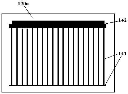
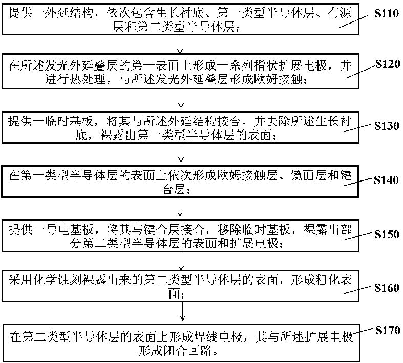
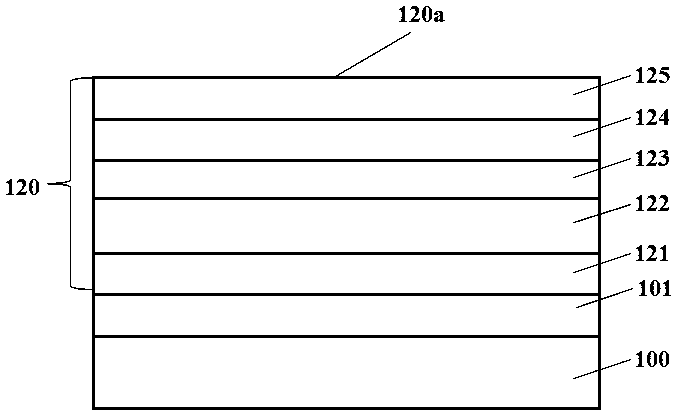
[0028] figure 2 It shows a flow chart of manufacturing a light-emitting diode according to the first preferred embodiment of the present invention, which mainly includes steps S110~S170. The following uses a quaternary light-emitting diode as an example in conjunction with the attached Figure 2~15 Describe in detail.

[0029] Step S110: providing a growth substrate 100 on which a light-emitting epitaxial ...


PUM


Abstract

The invention discloses a method for manufacturing a light-emitting diode, comprising the steps of: providing an epitaxial structure, which sequentially includes a growth substrate, a first-type semiconductor layer, an active layer, and a second-type semiconductor layer; Form extended electrodes on the substrate, and perform heat treatment to form ohmic contact with the second type semiconductor layer; provide a temporary substrate, bond it to the epitaxial structure, and remove the growth substrate to expose the surface of the first type semiconductor layer; An ohmic contact layer, a mirror layer, and a bonding layer are sequentially formed on the surface of the exposed first-type semiconductor layer; a conductive substrate is provided, bonded to the bonding layer, the temporary substrate is removed, and a part of the second semiconductor layer is exposed. The surface of the second type semiconductor layer and the extended electrode; use chemical etching to expose the surface of the second type semiconductor layer to form a roughened surface; form a welding wire electrode on the surface of the second type semiconductor layer, which forms a closed connection with the extended electrode circuit.

Description

technical field [0001] The invention relates to the field of semiconductor manufacturing, in particular to a light emitting diode and a manufacturing method thereof. Background technique [0002] Light-emitting diodes have good photoelectric characteristics such as low energy consumption, long life, good stability, small size, fast response speed and stable light-emitting wavelength, and are widely used in lighting, home appliances, display screens and indicator lights. [0003] With the development of substrate transfer technology, a p-type upward AlGaInP-based light-emitting diode appears, which removes the growth substrate through two substrate transfer techniques, and bonds a conductive substrate on the side of the n-type semiconductor, and on the surface of the p-type semiconductor Pad electrode 142 and extended electrode 141 are set on 120a. For high-power devices, the closed design of bonding wire electrode and extended electrode is often used, such as figure 1 shown...

Claims


Application Information

Patent Timeline
Patent Type & Authority Patents(China)
IPC IPC(8): H01L33/22H01L33/38
CPCH01L33/22H01L33/387H01L2933/0016H01L33/30H01L33/405H01L33/44H01L33/38H01L2933/0066H01L2933/0058
Inventor 蒙成吴俊毅杨恕帆王笃祥
Owner TIANJIN SANAN OPTOELECTRONICS
Why Eureka
Try Eureka