Light-emitting diode and manufacturing method thereof

A technology of light-emitting diodes and manufacturing methods, which is applied in the direction of electrical components, circuits, semiconductor devices, etc., can solve the problems of fragile metal contacts, affecting the roughening effect, side erosion, etc. The effect of increasing the coarsening ratio

Active Publication Date: 2017-05-31
TIANJIN SANAN OPTOELECTRONICS
View PDF8 Cites 3 Cited by
  • Summary
  • Abstract
  • Description
  • Claims
  • Application Information

AI Technical Summary

Problems solved by technology

However, the electrode material is generally magnetic. Since the welding wire electrode and the extended electrode form a series of closed loops, a certain magnetic field will be formed. During the roughening process, the charged particles in the roughening solution will move to cut the magnetic induction line, making the roughening solution Charged particles with different electrical properties are deflected in a certain direction in their respective magnetic fields, thus affecting the coarsening effect
At the same time, because the extended electrodes are not protected, side erosion often occurs, and the roughening solution etches to the bottom of the extended electrodes, resulting in the risk of fragile metal contacts or falling off

Method used


Image

  • Light-emitting diode and manufacturing method thereof
  • Light-emitting diode and manufacturing method thereof
  • Light-emitting diode and manufacturing method thereof

Examples


Embodiment Construction

[0027] The implementation of the present invention will be described in detail below with reference to the accompanying drawings and embodiments, so as to fully understand how the present invention applies technical means to solve technical problems and achieve the realization process of technical effects and implement them accordingly. It should be noted that, as long as there is no conflict, each embodiment of the present invention and each feature in each embodiment can be combined with each other, and the technical solutions formed are all within the protection scope of the present invention.

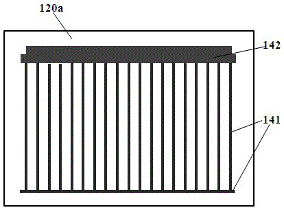
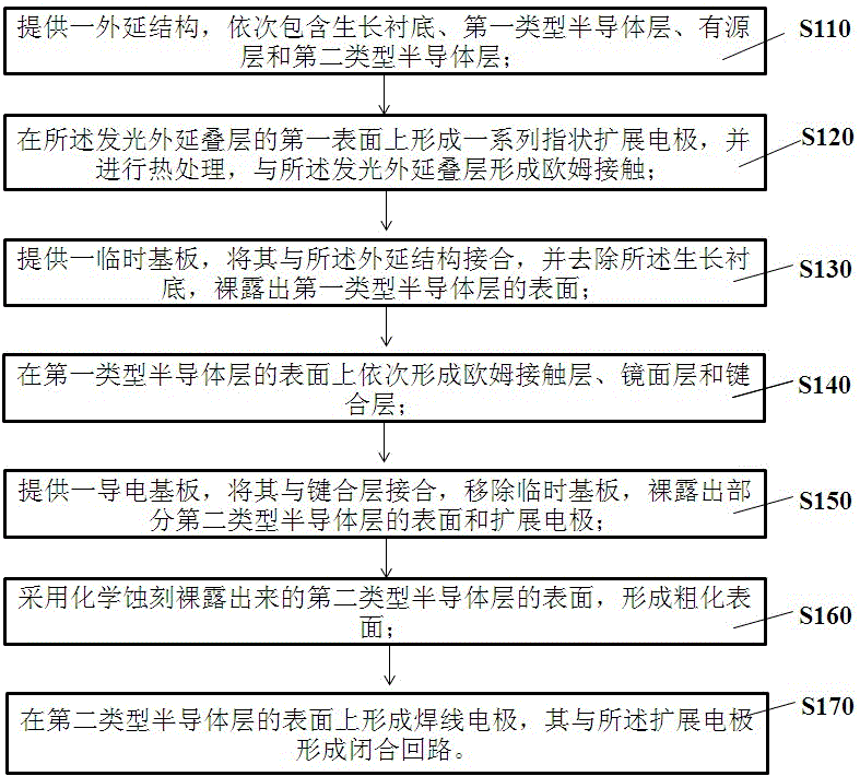
[0028] figure 2 Shows a production flow chart of a light-emitting diode according to the first preferred embodiment of the present invention, which mainly includes steps S110 to S170. The following takes a quaternary light-emitting diode as an example and attaches Figure 2~15 Give details.

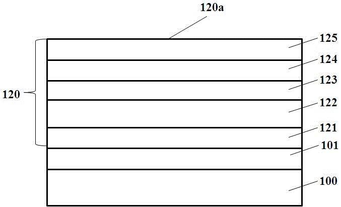
[0029] Step S110: Provide a growth substrate 100, and form a light-emitting epitaxial structure ...


PUM

PropertyMeasurementUnit
thicknessaaaaaaaaaa
widthaaaaaaaaaa
widthaaaaaaaaaa

Abstract

The invention discloses a manufacturing method of a light-emitting diode. The manufacturing method comprises the following steps: providing an epitaxial structure containing a growth substrate, a first-type semiconductor layer, an active layer and a second-type semiconductor layer in sequence; forming an expansion electrode on the surface of the second-type semiconductor layer, and carrying out heat treatment to form Ohmic contact with the second-type semiconductor layer; providing a temporary substrate, jointing the temporary substrate with the epitaxial structure, and removing the growth substrate, so that the surface of the first-type semiconductor layer is exposed; forming an Ohmic contact layer, a mirror surface layer and a bonding layer in sequence on the exposed surface of the first-type semiconductor layer; providing a conducting substrate, jointing the conducting substrate with the bonding layer, and removing the temporary substrate, so that the surface of the second-type semiconductor layer and the expansion electrode are exposed partially; chemically etching the exposed surface of the second-type semiconductor layer to form a coarse surface; and forming a bonding wire electrode on the surface of the second-type semiconductor layer, so that a closed circuit is formed by the bonding wire electrode and the expansion electrode.

Description

Technical field [0001] The invention relates to the field of semiconductor manufacturing, in particular to a light emitting diode and a manufacturing method thereof. Background technique [0002] Light-emitting diodes have good photoelectric characteristics such as low energy consumption, long life, good stability, small size, fast response speed and stable light-emitting wavelength, and are widely used in lighting, home appliances, display screens and indicator lights. [0003] With the development of substrate transfer technology, a p-type upward AlGaInP-based light-emitting diode appears, which removes the growth substrate through two substrate transfer techniques, and joins the conductive substrate on the n-type semiconductor side, on the surface of the p-type semiconductor A pad electrode 142 and an extended electrode 141 are arranged on 120a. For high-power devices, a closed design of wire bonding electrode and extended electrode is often used, such as figure 1 Shown. In the...

Claims


Application Information

Patent Timeline
Patent Type & Authority Applications(China)
IPC IPC(8): H01L33/22H01L33/38
CPCH01L33/22H01L33/387H01L2933/0016H01L33/30H01L33/405H01L33/44H01L33/38H01L2933/0066H01L2933/0058
Inventor 蒙成吴俊毅杨恕帆王笃祥
Owner TIANJIN SANAN OPTOELECTRONICS
Why Eureka
Try Eureka