InGaN/GaN quantum well laser and manufacturing method thereof

A manufacturing method and quantum well technology, applied to lasers, phonon exciters, laser components, etc., can solve problems such as thermal degradation, InGaN quantum well layer decomposition, and poor quality of GaN capping layers, and achieve good quality, In group evenly distributed effect

Active Publication Date: 2017-05-31
杭州增益光电科技有限公司
View PDF4 Cites 9 Cited by
  • Summary
  • Abstract
  • Description
  • Claims
  • Application Information

AI Technical Summary

Problems solved by technology

Regrown GaN cap layer on top of this 2D island topography, resulting in poor quality GaN cap layer
In addition, the InGaN quantum well active region with a high In composition has serious InGaN phase separation. After growing a low-temperature GaN cap layer with poor quality, the temperature rises to the barrier temperature and the high-temperature barrier growth process will lead to the decomposition of the InGaN quantum well layer.
When the high-temperature p-type AlGaN confinement layer of the laser structure is grown later, it will also cause thermal degradation in the active area of ​​the InGaN / GaN quantum well, and there are many dark spots in the fluorescence microscope photo

Method used


Image

  • InGaN/GaN quantum well laser and manufacturing method thereof
  • InGaN/GaN quantum well laser and manufacturing method thereof
  • InGaN/GaN quantum well laser and manufacturing method thereof

Examples


Embodiment Construction

[0020] Hereinafter, embodiments of the present invention will be described in detail with reference to the accompanying drawings. This invention may, however, be embodied in many different forms and should not be construed as limited to the specific embodiments set forth herein. Rather, the embodiments are provided to explain the principles of the invention and its practical application, thereby enabling others skilled in the art to understand the invention for various embodiments and with various modifications as are suited to particular intended uses.

[0021] In terms of the present invention, p-type means doped with Mg, u-type means undoped, n-type means doped with Si, etc.

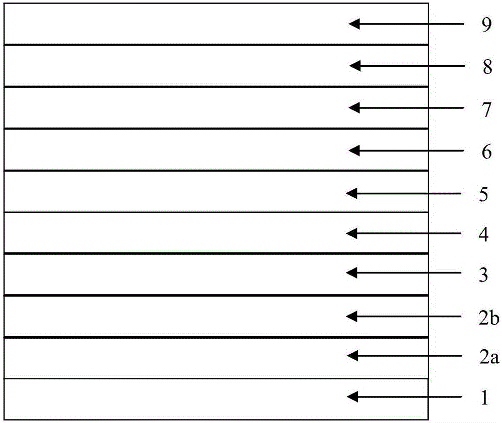
[0022] figure 1 is a schematic structural diagram of an InGaN / GaN quantum well laser according to an embodiment of the present invention.

[0023] refer to figure 1 , the InGaN / GaN quantum well laser according to an embodiment of the present invention comprises: a substrate 1; a low-temperature GaN...


PUM


Abstract

The invention discloses an InGaN / GaN quantum well laser, comprising a substrate and the following components sequentially arranged on the substrate: a low temperature GaN buffer layer, a high temperature n-type GaN layer and an n-type AlGaN light confinement layer; an n-type InGaN lower waveguide layer on the n-type AlGaN light confinement layer; an InGaN / GaN quantum well active region on the n-type InGaN lower waveguide layer; a u-type InGaN upper waveguide layer on the InGaN / GaN quantum well active region; a p-type AlGaN electron barrier layer on the u-type InGaN upper waveguide layer; a p-type AlGaN / GaN light confinement layer on the p-type AlGaN electron barrier layer; and a p-type GaN ohmic contact layer on the p-type AlGaN / GaN light confinement layer. The invention also discloses a manufacturing method for the InGaN / GaN quantum well laser. The invention adopts the InxGa1-XN of 1 to 2 single-atom layer thickness to be inserted into the cap layer so that the two-dimensional island-like surface of the InGaN quantum well surface becomes smooth, that the distribution of the In group becomes more uniform and that the subsequently formed GaN cap layer has a better quality in which the InGaN quantum well is not decomposed during the temperature rise and does not undergo thermal degradation during the subsequent high temperature growth of the p-type AlGaN / GaN light confinement layer.

Description

technical field [0001] The invention belongs to the technical field of semiconductors, and in particular relates to an InGaN / GaN quantum well laser and a manufacturing method thereof. Background technique [0002] GaN-based semiconductor lasers usually use InGaN / GaN quantum wells as the active region. Since the In-N bond energy is weak and the decomposition temperature is low, but the Ga-N bond energy is strong and the decomposition temperature is high, resulting in a large difference between the growth temperature of the optimal InGaN quantum well and the growth temperature of the optimal GaN quantum barrier. Therefore, we usually use the double temperature growth method to grow the InGaN / GaN quantum well active region, that is, the InGaN quantum well layer is grown at a lower temperature (generally lower than 750°C), and the GaN barrier layer is grown at a higher temperature (generally higher than 900°C). ℃). However, the InGaN quantum well layer often decomposes during ...

Claims


Application Information

Patent Timeline
Patent Type & Authority Applications(China)
IPC IPC(8): H01S5/343
CPCH01S5/34333
Inventor 田爱琴刘建平张书明李德尧张立群杨辉
Owner 杭州增益光电科技有限公司
Why Eureka
Try Eureka